

Ijraset Journal For Research in Applied Science and Engineering Technology
Design of CMOS Circuit Based on NAND Function at 150nm Channel Length for Low-Power and High-Speed IC Fabrication
Authors: Spandan Roy, Swastik Roy, Arpan Adhikary, Anilesh Dey, Sandhya Pattanayak, Surajit Bari
DOI Link: https://doi.org/10.22214/ijraset.2022.44299
Certificate: View Certificate
Abstract
In this paper the low-power and high-speed design approach of one Complementary Metal Oxide Semiconductor (CMOS) circuit based on NAND function has been reported. The CMOS design methodology has been followed to construct the circuit. The design has been carried out at 150 nm channel length of Metal Oxide Semiconductor (MOS) transistor. Average power consumption and gate delay of the circuit has been measured. Power-delay product (PDP) of the circuit has been calculated for optimized operation. The simulation of the circuit has been carried out with the help of Tanner SPICE (T-SPICE) software.
Introduction
I. INTRODUCTION
CMOS design technique is the simplest methodology [1-4] for integrated circuit design. In this method two blocks are used. The block which is connected between power supply voltage and output is known as pull-up network (PUN) and the block which is connected between the output node and ground is known as the pull-down network (PDN) [5-6]. Whenever, PUN is on then logic “1” is transferred to the output node and during this time some power is dissipated across PUN [3-4]. On the other hand, whenever PDN is on, logic “0” is transferred to the output node and some power is dissipated in across the PDN. This type of power dissipation is known as switching or dynamic power dissipation [7-10]. In addition to the switching power, short circuit power and leakage power dissipation are also observed in CMOS circuit [1-4]. Therefore, average power consumption is the summation of switching power, short circuit power and leakage power dissipation. Low-power & high-speed circuit design is the recent trends of Integrated Circuit fabrication [11-15] In this work, the two input CMOS NAND gate has been constructed. Context to the low power and high-speed integrated circuit fabrication, the power consumption & delay of the CMOS NAND gate has been measured and reported.
II. DESIGN OF TWO INPUT CMOS NAND FUNCTION USING SPICE
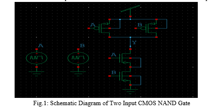
The schematic diagram of two input CMOS NAND gate is shown in Fig.1. Two NMOS transistors are connected in series in the pull-down network. Two PMOS transistors are connected in parallel in the pull-up network. To avoid the body bias effect, body terminal is connected to the source terminal. The source terminals of PMOS transistors are connected to power supply voltage (VDD) and source terminal of one of the NMOS transistor is connected to ground. Two-bit sources are used for the generation of the input signal. The node “A” and “B” are considered as input terminals and node “Y” has been considered as output terminal.
III. CLARIFICATION OF FUNCTIONALITY OF CMOS NAND GATE
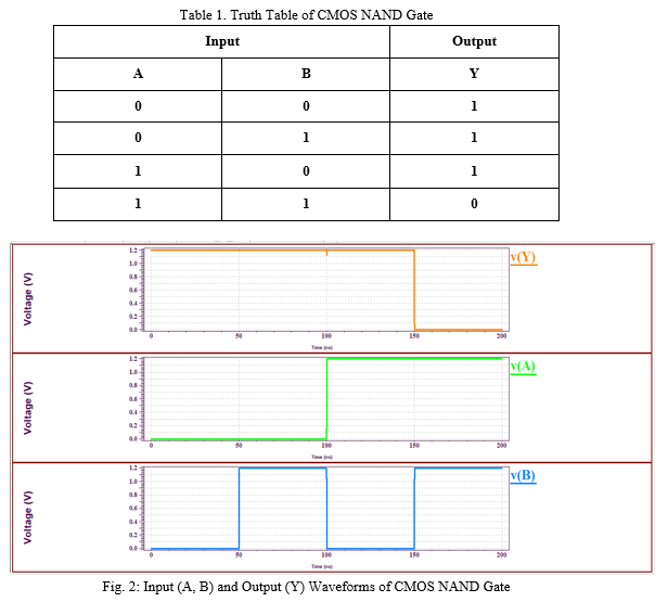
For the correctness of the design, the netlist of the circuit has been generated and simulated at 150 nm channel length of MOS transistor. For the clarification of the functionality of the CMOS NAND gate, the truth table of the CMOS NAND gate is shown in table1. The input and output waveforms are shown in Fig.2. As shown in Fig.2, the output is logic “High”, whenever any of the input is at logic “Zero”. However, when all the inputs are at logic “High” output transits to logic “Zero”. The simulated waveforms as shown in Fog.2 is like the bit patterns according to the truth table of Table.1. This indicates the correct functionality of the circuit.
IV. AVERAGE POWER CONSUMPTION, SPEED AND PDP ANALYSIS OF CMOS NAND GATE AT 150 NM CHANNEL LENGTH OF MOS TRANSISTOR
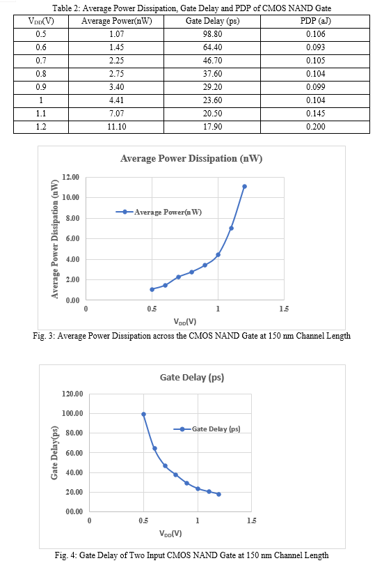
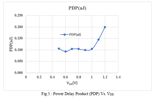
The average power consumption, gate delay of the CMOS NAND gate has been measured and presented in Table 2. The Power-Delay Product (PDP) of the circuit has also been calculated and shown in Table 2. The graph related to average power consumption is shown in Fig.3. The power dissipation in the circuit increases with increasing VDD. Therefore, to reduce the power consumption the VDD needs to be scaled down. The graphical variation of delay is shown in Fig.4. It is found that, the gate delay decreases for the higher value of VDD. Therefore, reference to Fig. 3 and 4, it is contradictory regarding the value of VDD for which the performance is acceptable. To get the optimum value of VDD, the PDP has been calculated. The graphical variation of PDP is shown in Fig.5. From Fig.5, it has been observed that in between 1 Volt and 1.2 Volt of VDD, at 0.6 V, 0.7 V and 0.9 V PDPs are supposed to be optimum.
Conclusion
In this work, the two input CMOS NAND gate has been designed at 150 nm channel length of MOS transistor. The functionality of the circuit has been verified. Average power consumption and gate delay of the circuit has been measured and reported. Power dissipation increases with increasing VDD but gate delay decreases that is speed of response increases with increasing VDD.. For better operation power-delay product has been calculated and plotted. It is found that within the range of 0.5 V to 1.2 V of VDD, at 0.6 V ,0.7 V and 0.9 V PDP is supposed to be optimum with values 0.096 aJ, 0.105 aJ and 0.099 aJ respectively. The values of PDP, average power consumption and gate-delay are very small in this work. Therefore, results in this work are considerable for low-power and high-speed integrated circuit design and fabrication.
References
[1] Rabaey J, Chandrakasan A, Nikolic B “Digital integrated circuits a design perspective”. Pearson, London,2005 [2] Sarkar A, De S, Sarkar CK “VLSI design and EDA tools”. Scitech Publications (India) Pvt Ltd, Chennai,201 [3] Kang SM, Leblebici Y “CMOS digital integrated circuits analysis and design”. T.M.H., New Delhi,2003 [4] Uyemura J “Introduction to VLSI circuits and systems”. Willey, India,2007 [5] Shibata N, Gotoh Y “High-density RAM/ROM macros using CMOS Gate-array base cells: hierarchical verification technique for reducing design cost”. IEEE Trans Very Large Scale Integr VLSI Syst 23:1415–1428,2015 [6] Salivahanan S, Arivazhagan S “Digital circuits and design”. Vikas Publishing House Pvt. Ltd., Noida,2007 [7] Jain RP “Modern digital electronics. TMH, New Delhi ,2002 [8] Chhabra A, Rawat H, Jain M, Tessier P, Pierredon D, Bergher L,Kumar P “FALPEM: framework for architectural-level power estimation and optimization for large memory subsystems”. Trans Comput Aided Des Integr Circuits Syst 34:1138–1142. doi:10.1109/TCAD.2014.2387859,2015 [9] Deepa S, Kumar SV “Analysis of low power 1-bit adder cells using different XOR-XNOR gates”. In: IEEE international conference on computational intelligence & communication technology (CICT), 2015. doi:10.1109/CICT.2015.21 [10] Chi-Wa U;Man-Kay Law;Chi-Seng Lam;Rui P. Martins “Switched-Capacitor Bandgap Voltage Reference for IoT Applications” IEEE Transactions on Circuits and Systems, Volume: 69, Issue: 1, 2022 [11] Ricardo Martins;Nuno Lourenço;Nuno Horta;Shenke Zhong;Jun Yin;Pui In Mak;Rui P. Martins “Design of a 4.2-to-5.1 GHz Ultralow-Power Complementary Class-B/C Hybrid-Mode VCO in 65-nm CMOS Fully Supported by EDA Tools” IEEE Transactions on Circuits and Systems, Volume: 67, Issue: 11,2020 [12] Luheng Jia;Chi-Ying Tsui;Oscar C. Au;Kebin Jia “A Low-Power Motion Estimation Architecture for HEVC Based on a New Sum of Absolute Difference Computation” IEEE Transactions on Circuits and Systems for Video Technology, Volume: 30, Issue: 1, 2020 [13] Venkat Subba Rao. Manchala;G Ramana Murthy “Low-Power and Low-Leakage Design Techniques in CMOS Technology” 5th International Conference on Trends in Electronics and Informatics (ICOEI),2021 [14] Soumya Kayala;K. Vasanth “Low Power VLSI Architecture for Data Comparators for Non-Linear Imaging Applications” International Conference on Innovative Computing, Intelligent Communication and Smart Electrical Systems (ICSES),2021 [15] K. Gavaskar;D. Malathi;R. Dhivya;R. Dimple Dayana;I. Dharun “ Low Power Design of 4-bit Simultaneous Counter using Digital Switching Circuits for Low Range Counting Applications” 5th International Conference on Devices, Circuits and Systems (ICDCS),2020
Copyright
Copyright © 2022 Spandan Roy, Swastik Roy, Arpan Adhikary, Anilesh Dey, Sandhya Pattanayak, Surajit Bari. This is an open access article distributed under the Creative Commons Attribution License, which permits unrestricted use, distribution, and reproduction in any medium, provided the original work is properly cited.

Download Paper
Paper Id : IJRASET44299
Publish Date : 2022-06-15
ISSN : 2321-9653
Publisher Name : IJRASET
DOI Link : Click Here
 Submit Paper Online