

Ijraset Journal For Research in Applied Science and Engineering Technology
Development of a Bidirectional DC/DC Converter with Dual-Battery Energy Storage for a Hybrid Electric Vehicle System
Authors: Mr. Bure Raju, Dr. S. Sivaganesan
DOI Link: https://doi.org/10.22214/ijraset.2023.49579
Certificate: View Certificate
Abstract
This study develops a newly designed, patented, bidirectional DC/DC converter (BDC) that interfaces a main energy storage (ES1), an auxiliary energy storage (ES2), and a DC-bus of different voltage levels, for application in hybrid electric vehicle systems. The proposed converter can operate in a step-up mode (i.e., low-voltage dual-source-powering mode) and a step-down (i.e., high-voltage dc-link energy-regenerating mode), both with bidirectional power flow control. In addition, the model can independently control power flow between any two low-voltage sources (i.e., low-voltage dual-source buck/boost mode). Herein, the circuit configuration, operation, steady-state analysis, and closed-loop control of the proposed BDC are discussed according to its three modes of power transfer.
Introduction
I. INTRODUCTION
Here a lot of research conducted on hybrid electric vehicles (HEVs), electric vehicles (EVs), and plug-in hybrid electric vehicles (PHEVs) due to the environmental and economic concerns in which hybrid energy storage systems (HESSs) have been comprehensively studied. The aim of a HESS is to make use of strong features of ESS elements while eliminating their weaknesses to reach the performance of an ideal ESS element. In order to create a HESS having the characteristics of an ideal energy storage unit such as high energy/power density, low cost/weight per unit capacity, and long cycle life, researchers have hybridized batteries and ultra capacitors (UCs) the active hybridization of the aforementioned ESSs, in which the power/current of the ESS can be controlled fully, is only possible by means of utilizing power converters. Manuscript received July 3, 2015; revised October 5,2015, accepted October 27, 2015. Power converter topologies used in HESS can be classified into two main categories, i.e., isolated and non-isolated. In, isolated HEES system topologies include a transformer to offer galvanic isolation between sources and output. Non-isolated power converters are much simpler in terms of design and control when compared to isolated ones.
One of the simplest way to build a non-isolated HESS is to connect some of the sources directly while linking others to dc bus via bidirectional dc-dc converters as in; however, this method does not allow to adjust the dc bus voltage. In addition, studies in propose individual dc-dc converters for each input. Unlike the former topology, the multiple converter topology structure enables managing the output voltage; however, it is an expensive approach as it requires multiple converters. In order to decrease the cost of multiple converter topologies, multi input converter (MIC) topologies are reported in the literature. As mentioned in, MICs are not only cost-effective; but also reliable, simple, and easy to control. In, a bidirectional MIC having a single inductor shared by input sources is proposed; although this converter has the advantage of being simple, unfortunately, it does not allow active power sharing between sources. In, authors offer a multi input dc-dc/ac boost converter which contains a bidirectional port for battery storage in addition to several unidirectional ports for dc sources; therefore, it can be asserted that this converter does not offer flexibility in terms of the number of EES elements. In , authors suggest a bidirectional MIC called multiple input power electronics converter (MIPEC) whose input ports connected to dc bus via half bridges as shown in Fig.1(a); it can successfully control charge/discharge currents of input sources whose voltages are required to be less than the output voltage. In, a modified boost converter is introduced; this converter is constructed in a way that the classical boost converter inductor is replaced with a coupled inductor and a high valued capacitor; here, the input current ripple is aimed to be eliminated via a single switch driving the input source energy and energy stored in the capacitor.
Based on this concept, a non-isolated unidirectional double input dc-dc power converter is proposed in. In this paper, instead of the high valued capacitor in, the author utilized an EES element, namely a UC, which is essentially a capacitor with large capacitance.
The motivation of is to create an global climate change and energy supply is declining have stimulated changes in vehicular technology. Advanced technologies are currently being researched for application in future vehicles. Among such applications, fuel-cell hybrid electric vehicles (FCV/HEV) are efficient and promising candidates. In the past. Studied the vehicles’ dynamics to look for an optimal torque-speed profile of the electric propulsion system.. Discussed the operating properties of the topologies for different vehicles including HEV, FCV, and more electric vehicles. also integrated power electronics intensive solutions in advanced vehicular power system to satisfy huge vehicular load . sufficiently divide the load power among the fuel cell stack, the battery, and the ultra capacitors based on two proposed energy-management strategies. studied the influence of fuel-cell (FC) performance and the advantages of hybridization for control strategies. reviewed electric, hybrid, and fuel-cell vehicles and focused on architectures and modeling for energy management. presented energy-storage topologies for HEVs and plug-in HEVs (PHEVs). They also discussed and compared battery, UC, and FC technologies. Furthermore, they also addressed various hybrid ESSs that integrate two or more storage devices. the current status and the requirements of primary electric propulsion components-the battery, the electric motors, and the power electronics system. implemented a bidirectional dc/dc converter topology with two-phase and interleaved characteristics. For EV and dc-micro grid systems, the converter has an improved voltage conversion ratio. Furthermore, Lai also studied a bidirectional dc to dc converter (BDC) topology which has a high voltage conversion ratio for EV batteries connected to a dc-micro grid system. In FCV systems, the main battery storage device is commonly used to start the FC and to supply power to the propulsion motor. The battery storage devices improve the inherently slow response time for the FC stack through supplying peak power during accelerating the vehicle. Moreover, it contains a high power-density component such as super capacitors (SCs) eliminates peak power transients during accelerating and regenerative braking . In general, SCs can store regenerative energy during deceleration and release it during acceleration, thereby supplying additional power. The high power density of SCs prolong the life span of both FC stack and battery storage devices and enhances the overall efficiency of FCV systems.
A functional diagram for a typical (FCV/HEV) power system is illustrated in Fig. The low-voltage FC stack is used as the main power source, and SCs directly connected in parallel with FCs. The dc/dc power converter is used to convert the FC stack voltage into a sufficient dc-bus voltage in the driving.
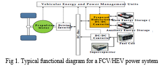
Inverter for supplying power to the propulsion motor. Furthermore, ES1 with rather higher voltage is used as the main battery storage device for supplying peak power, and ES2 with rather lower voltage could be an auxiliary battery storage device to achieve the vehicle range extender concept. The function of the bidirectional dc/dc converter (BDC) is to interface dual-battery energy storage with the dc-bus of the driving inverter.
Generally, the FC stack and battery storage devices have different voltage levels. Several multiport BDCs have been developed to provide specific voltages for loads and control power flow between different sources, thus reducing overall cost, mass, and power consumption. These BDCs can be categorized into isolated and nonisolated types.
In isolated converters, high-frequency power transformers are applied to enable galvanic isolation. A few isolated multiport BDC topologies have been investigated, such as the fly-back, half- or full-bridge circuits, dual-active bridges, and resonant circuits.The literature suggests that non-isolated BDCs are more effective than typical isolated BDCs in EVs derived non-isolated multi-input converter topologies by way of a combination of buck, boost, ?uk, and Sepic. In, developed the three-port non-isolated multi-input-multi-output (MIMO) converter topologies for interfacing a renewable source, a storage battery, and a load simultaneously. The three double-input converters developed in comprise a single-pole triple-throw switch and only one inductor. A modular nonisolated MIMO converter was presented in.
This converter is applied to hybridize clean energy sources of EVs and the basic boost circuit was modified and integrated. However, the voltage gain of the MIMO boost circuit is limited in practice, because of the losses associated with some components such as the main power switch, inductor, filter capacitor, and rectifier diode. To overcome this drawback, three-port power converter that has high-gain characteristic and contains FC, battery sources and stacked output for interfacing HEV, as well as a dc-microgrid was presented [27]. Although the multiport BDC discussed in [25] can interface more than two sources of power and operate at different voltage levels, it still has limited static voltage gains, resulting in a narrow voltage range and a low voltage difference between the high-and low-side ports.
This study proposes a new BDC topology for FCV/HEV power systems that consists of an interleaved voltage-doubler structure [9, 28] and a synchronous buck-boost circuit. It features two main operating modes: a low-voltage dual-source-powering mode and a high-voltage dc-bus energy-regenerating mode. In addition, the proposed converter can independently control power flow between any two low-voltage sources when in the low-voltage dual-source buck/boost mode. A similar topology was introduced in [29] that only describes a brief concept. By contrast, this study presents a detailed analysis of the operation and closed-loop control of this new topology as well as simulation and experimental results for all its modes of operation. Moreover, this study expanded the topology presented in [29] because the proposed converter can operate over a wider range of voltage levels. The main characteristics of the proposed converter are summarized as follows:
- Interfaces more than two dc sources for different voltage levels
- Controls power flow between the dc bus and the two low-voltage sources and also independently controls power flow between the two low-voltage sources
- Enhances static voltage gain and thus reduces switch voltage stress
- Possesses a reasonable duty cycle and produces a wide voltage difference between its high- and low-side ports.
II. PROPOSED TOPOLOGY AND OPERATION MODES
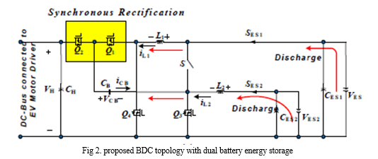
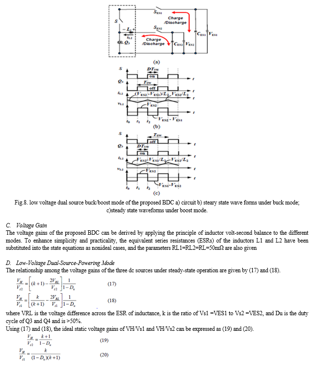
The proposed BDC topology with dual-battery energy storage is illustrated in Fig. 5.1, where VH, VES1, and VES2 represent the high-voltage dc-bus voltage, the main energy storage (ES1), and the auxiliary energy storage (ES2) of the system, respectively. Two bidirectional power switches (SES1 and SES2) in the converter structure, are used to switch on or switch off the current loops of ES1 and ES2, respectively. A charge-pump capacitor (CB) is integrated as a voltage divider with four active switches (Q1, Q2, Q3, Q4) and two phase inductors (L1, L2) to improve the static voltage gain between the two low-voltage dual sources (VES1, VES2) and the high-voltage dc bus (VH) in the proposed converter. Furthermore, the additional CB reduces the switch voltage stress of active switches and eliminates the need to operate at an extreme duty ratio. Furthermore, the three bidirectional power switches (S, SES1, SES2) displayed in Fig. 2 exhibit four-quadrant operation and are adopted to control the power flow between two low-voltage dual sources (VES1, VES2) and to block either positive or negative voltage. This bidirectional power switch is implemented via two metal-oxide-semiconductor field-effect transistors (MOSFETs), pointing in opposite directions, in series connection.
To explain the concept for the proposed converter, all the conduction statuses of the power devices involved in each operation mode are displayed in Table I. Accordingly, the four operating modes are illustrated as follows to enhance understanding.
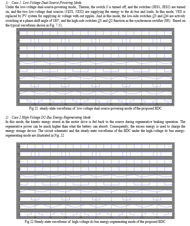
A. Low-Voltage Dual-Source-Powering Mode
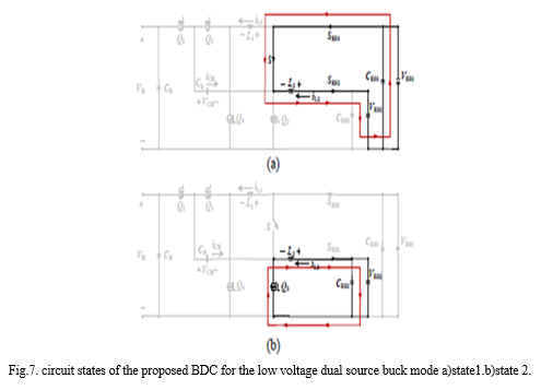
Fig. 5.2(a) depicts the circuit schematic and steady-state waveforms for the converter under the low-voltage dual-source-powering mode. Therein, the switch S is turned off, and the switches (SES1, SES2) are turned on, and the two low-voltage dual sources (VES1, VES2) are supplying the energy to the dc-bus and loads. In this mode, the low-side switches Q3 and Q4 are actively switching at a phase-shift angle of 180°, and the high-side switches Q1 and Q2 function as the synchronous rectifier (SR).
Based on the typical waveforms shown in Fig. 5.2(b), when the duty ratio is larger than 50%, four circuit states are possible (Fig.5.2). In the light of the on/off status of the active switches and the operating principle of the BDC in low-voltage dual-source-powering mode, the operation can be explained briefly as follows.
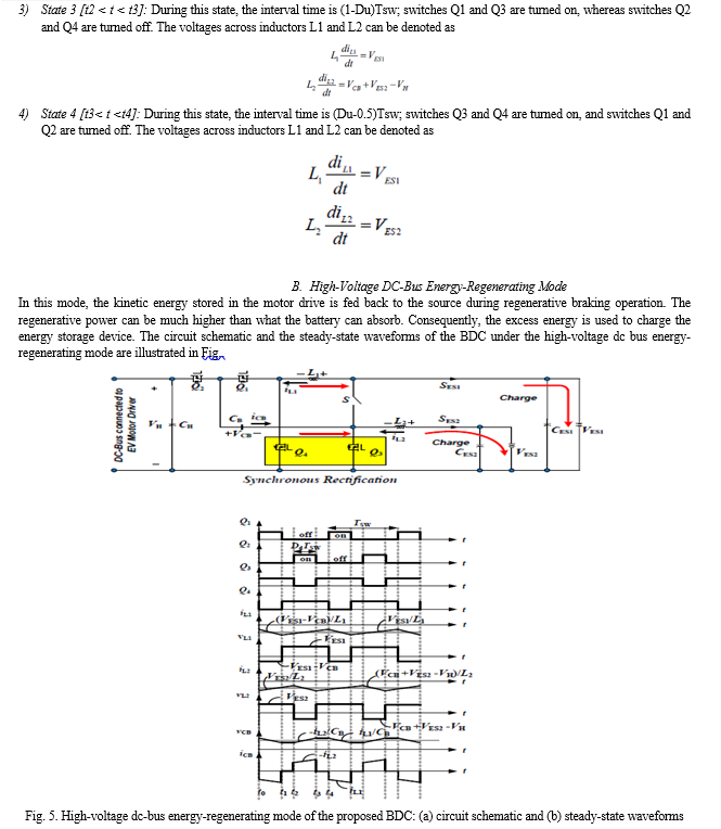
- State 1 [t0 < t < t1]: During this state, the interval time is (1-Du)Tsw, switches Q1, Q3 are turned on, and switches Q2, Q4 are turned off. The voltage across L1 is the difference
Between the low-side voltage VES1 and the charge-pump voltage (VCB), and hence iL1 decreases linearly from the initial value. In addition, inductor L2 is charged by
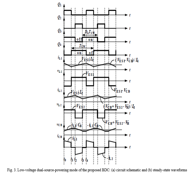
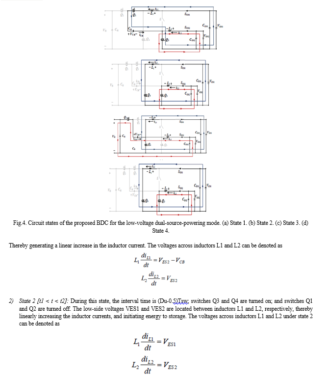
Therein, the current in the inductors is controlled by the active switches Q1 and Q2, which have a phase-shift angle of 180° and thereby direct the flow away from the dc-bus and toward the dual energy storage devices; the switches Q3 and Q4 function as the SR to improve the conversion efficiency.
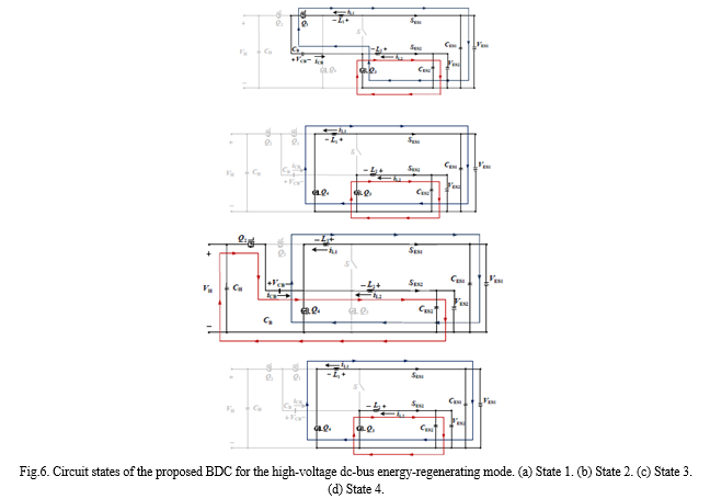
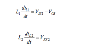
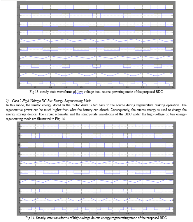
On the basis of the steady-state waveforms shown in Fig. 5(b), when the duty ratio is below 50%, four different circuit states are possible, as shown in Fig. 6. In the light of the on-off status of the active switches and the operating principle of the BDC in high-voltage dc-bus energy-regenerating mode, the operation can be depicted briefly as follows.
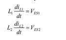
- State 1 [t0 < t < t1]: During this state, the interval time is DdTsw; switches Q1 and Q3 are turned on, and switches Q2 and Q4 are turned off. The voltage across L1 is the difference between the low-side voltage VES1 and the charge-pump voltage VCB; hence, the inductor current iL1 decreases linearly from the initial value. In addition, inductor L2 is charged by the energy source VES2, which also contributes to the linear increase in the inductor current. The voltages across inductors L1 and L2 can be denoted as
2. State 2 [t1 < t < t2]: During this state, the interval time is (0.5-Dd)Tsw; switches Q3 and Q4 are turned on, and switches Q1 and Q2 are turned off. The voltages across inductors L1 and L2 are the positive the low-side voltages VES1 and VES2, respectively; hence, inductor currents iL1 and iL2 increase linearly. These voltages can be denoted as
3. State 3 [t2 < t < t3]: During this state, the interval time is DdTsw; switches Q1 and Q3 are turned off, and switches Q2 and Q4 are turned on. The voltage across L1 is the positive low-side voltage VES1 and hence iL1 increases linearly from the initial value. Moreover, the voltage across L2 is the difference of the high-side voltage VH, the charge-pump voltage VCB, and the low-side voltage VES2, and its level is negative. The voltages across inductors L1 and L2 can be denoted as
4. State 4 [t3 < t < t4]: During this state, the interval time is (0.5-Dd)Tsw; switches Q3 and Q4 are turned on, and switches Q1 and Q2 are turned off. The voltages across inductors L1 and L2 can be denoted as

???????C. Low-Voltage Dual-Source Buck/Boost Mode
The circuit schematic for this mode, which involves the transfer of energy stored in the main energy storage to the auxiliary energy storage and vice versa is presented in Fig. Therein, the topology is converted into a single-leg bidirectional buck-boost converter.As shown in Fig, when the duty cycle of the active bidirectional switch S is controlled, the buck converter channels power from main energy storage to the auxiliary energy storage. By contrast, when the duty cycle of switch Q3 is controlled, power flows from the auxiliary energy storage to main energy storage, indicating that the converter is operating in boost mode, as illustrated in Fig.
III. BIDIRECTIONAL DC TO DC CONVERTER
A conventional buck-boost converter can management the power flow in one direction only but power can flow in both the direction in bidirectional converter. Bidirectional dc-dc converters are the device for the purpose of step-up or step-down the voltage level with the capability of flow power in either forward directions or in backward direction. Bidirectional dc-dc converters work as regulator of power flow of the DC bus voltage in both the direction. In the power generation by wind mills and solar power systems, output fluctuates because of the changing environment condition. These energy systems are not reliable to feed the power as a standalone system because of the large fluctuations in output and hence these energy system systems are always connected with energy storage devices such as batteries and super capacitors Fig. 1(b). These energy storage devices store the surplus energy during low load demand and provide backup in case of system failure and when the output of energy system changes due to weather conditions. Thus, a bidirectional dc-dc converters are needed to allow power flow in both forward and backward the directions. A conventional dc-dc converter can be converted into a bidirectional converter using bidirectional switch by using diode in anti-parallel with MOSFET or IGBT allowing current flow in both the direction using controlled switching operation.
???????A. Types of Bidirectional Converter
There are two types of Bi-directional dc/dc converter on the basis of galvanic isolation provided between input and output [19].
- NIBDC
- IBDC
a. Non-Isolated Bidirectional Dc to Dc Converter (NIBDC): NIBDC is a converter which does not use high frequency transformer to provide any electrical isolation between source and load. Hence these converters are not used in high power applications due to safety reasons but in low power application theses converter are more efficient because these are easy to control and light weight due to absence of transformer.
b. Bidirectional Buck-boost Converter: This topology is basic circuit of bidirectional dc-dc converter Fig. It is the anti-parallel combination of buck-boost converters. During the step-up operation Q1 is conduct according to the duty cycle whereas Q2 will not conduct in this mode. In step- down mode Q2 will conduct according to the duty cycle and Q1 will not conduct in this mode. A small dead time provided between both the operation so that cross conduction can be avoided . Given topology is a non-isolated half-bridge BDC topology and it is designed by the combination of boost converter connected anti parallel with buck converter. This topology is simple and has greater efficiency.
c. Cascaded Bidirectional Buck-boost Converter: This topology Fig. 5.2(d) is obtained by cascading buck converter with boost converter . With this topology all four quadrant is possible hence this topology works as buck mode and boost mode in both the direction. 4-quardant operation of this topology makes this topology most flaxible but it has some limitations also: more number of switches which leads to more switching losses, complex control algorithm and more turn-on losses because of reverse recovery of diodes.
d. Bidirectional CUK Converter: Bidirectional CUK converter [25] is obtained from unidirectional CUK converter by using MOSFET in place of diode Fig. The output of this converter has low ripple as compared to above described topologies hence this converter can be a better option for interfacing super-capacitor-battery in circuits . The ripple output current can be reduced by coupling of inductor L1and L2. In the forward power flow, Q1 works as controlled switch and Q2 remain off and body diode of switch Q2 works as main diode. Similarly, in backward power flow Q2 works as controlled switch and Q1 remain off and body diode of switch Q1 works as main diode.
???????B. Steady-State Analysis
In this section, we analyze the voltage gain, switch voltage stress, and uniform average current sharing characteristics of the proposed BDC when operating.
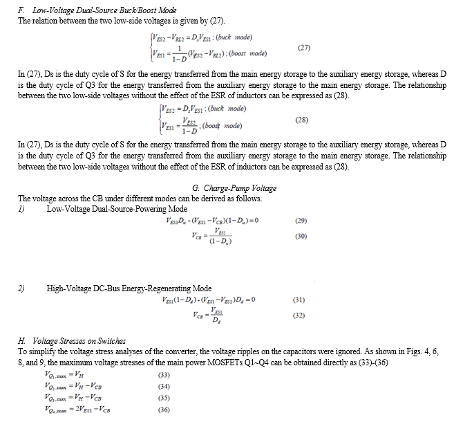
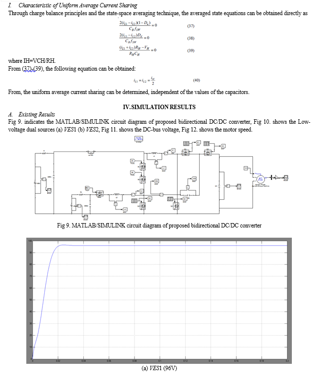
Although these voltage gains are reduced by the ESR of the inductors under the nonideal situation, the parasitic effect is relatively small and thus the reduced voltage gain can be easily compensated for by increasing the duty control. In order to test the dynamic performance of the system, a load profile is chosen according to normalized ECE-15 driving cycle [25]; the analyzed section of this driving cycle is demonstrated in Fig,. This period is chosen to examine the system under maximum power demand and in the presence of regenerative braking energy. The load profile is created by utilizing dc load bank and dc generator which are shown in Fig.
Moreover, simulations are carried out via developed PSIM switching model including switch turn-ON resistances and output capacitor equivalent serial resistance; in the simulation, battery and UC are modeled as in. Note that in both cases battery and UC initial voltages are set to 38 V and 33.6 V (70% state-of-charge), respectively. Figs. 19-21 compare the experimental and simulation results. In Fig, the output voltage and output current are shown. Here, it is clear that the output voltage is successfully regulated at 48 V in both cases. Moreover, the fact that output current in the experiment and simulation match well indicates that the output power is adjusted as intended by load bank and generator Fig. shows the battery and UC average current. From Fig. 20, it can be noticed that the battery current variations in the experiment and in the simulation appear similar. In both cases maximum battery current is limited to 20 A due to the control strategy; at this instant, UC current is increased for compensating the load demand. Additionally, UC current becomes negative when it stores regenerative braking energy.Fig. highlights the input source voltages. This figure indicates that battery voltage as well as UC voltage in the experiment and in the simulation change in a similar way. Because of its equivalent serial resistance, battery voltage decreases substantially when it gives power. In addition to that, UC voltage decreases when it compensates load demand and increases when it is charged.
The voltage and current of Q0 body diode are illustrated in one can see that when T0 is OFF, the diode starts to conduct as can be understood from its positive current. Conversely, when S0 is ON, the diode becomes OFF thus its current goes to zero. Illustrate the measured steady state waveforms when the converter operates in the charging mode. In this test, by controlling Q0 switch, the output voltage is again kept at 48 V while UC is charged under 400W constant power. Based on these figures, it can be asserted that the experimental results match the theoretical waveforms given in Fig. 4. Fig. 15 shows the experimental results of Q0 terminal voltages at steady state. In Fig.15, the duty cycle of Q0 is about 0.8 as expected according to (10) which explains the relationship between the duty cycle of Q0, UC voltage (~40V), and the output voltage. Figs. 15-16 illustrate the measured steady state waveforms when the converter operates in the charging mode. In this test, by controlling Q0 switch, the output voltage is again kept at 48 V while UC is charged under 400W constant power.
Based on these figures, it can be asserted that the experimental results match the theoretical waveforms given in Fig. 5.3. Fig. shows the experimental results of Q0 terminal voltages at steady state. In Fig., the duty cycle of Q0 is about 0.8 as expected according to (10) which explains the relationship between the duty cycle of Q0, UC voltage (~40V), negative since UC is charged. Moreover, when Q0 is turned ON, the voltage of the inductor becomes negative thus its current increases (negatively); conversely, turning it OFF makes the voltage of the inductor equal to UC voltage and decreases its current (negatively). Fig illustrates the proposed converter efficiency curves for the discharging and charging modes which are obtained by power analyzer. In the discharging mode, the power of one source is set to 200 W while other source is utilized to compensate the load demand. Besides, in the charging mode,dc bus is regulated when adjusting the charging power of the and the output voltage In Fig., the voltage and current variations of L2 are demonstrated. It can be noticed that the inductor current
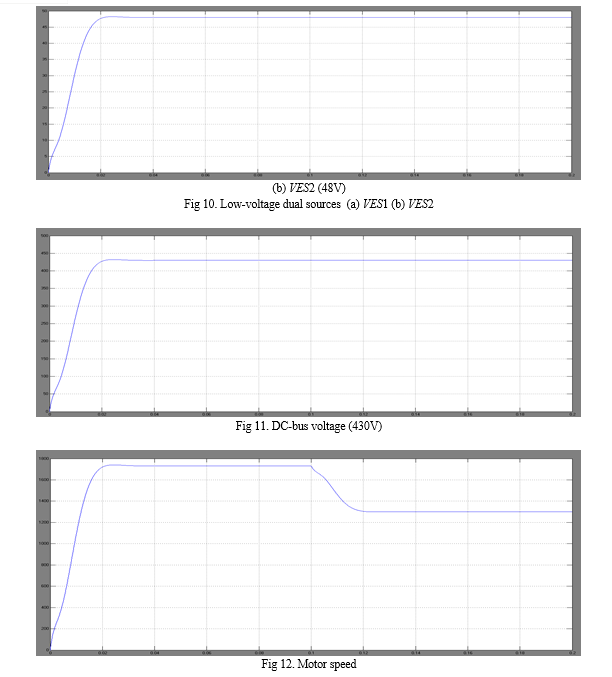
1) Case 1: Low-Voltage Dual-Source-Powering Mode
Under the low-voltage dual-source-powering mode. Therein, the switch S is turned off, and the switches (SES1, SES2) are turned on, and the two low-voltage dual sources (VES1, VES2) are supplying the energy to the dc-bus and loads. In this mode, the low-side switches Q3 and Q4 are actively switching at a phase-shift angle of 180°, and the high-side switches Q1 and Q2 function as the synchronous rectifier (SR). Based on the typical waveforms shown in Fig. 13.,
 ???????
Conclusion
The solar cells collect a portion of the sun‘s energy and store it into the batteries of the solar car. Before that happens, power trackers converts the energy collected from the solar array to the proper system voltage, so that the batteries and the motor can use it. After the energy is stored in the batteries, it is available for use by the motor & motor controller to drive the car. We are going to use two set of batteries; one of which will get the electrical energy from the panel to drive the motor and another will be used as auxiliary power source which will provide required power to other electrical devices being used in the vehicle. A new PV based BDC topology was presented to interface dual battery energy sources and high-voltage dc bus of different voltage levels. The circuit configuration, operation principles, analyses, and static voltage gains of the proposed BDC were discussed on the basis of different modes of power transfer. Simulation and experimental waveforms for a 1 kW prototype system highlighted the performance and feasibility of this proposed BDC topology. The highest conversion efficiencies were 97.25%, 95.32%, 95.76%, and 92.67% for the high-voltage dc-bus energy-regenerative buck mode, low-voltage dual-source-powering mode, low-voltage dual-source boost mode (ES2 to ES1), and low-voltage dual-source buck mode (ES1 to ES2), respectively. The results demonstrate that the proposed BDC can be successfully applied in FC/HEV systems to produce hybrid power architecture.
References
[1] M. Ehsani, K. M. Rahman, and H. A. Toliyat, \"Propulsion system design of electric and hybrid vehicles,\" IEEE Transactions on industrial electronics, vol. 44, no. 1, pp. 19-27, 1997. [2] A. Emadi, K. Rajashekara, S. S. Williamson, and S. M. Lukic, \"Topological overview of hybrid electric and fuel cell vehicular power system architectures and configurations,\" IEEE Transactions on Vehicular Technology, vol. 54, no. 3, pp. 763-770, 2005. [3] A. Emadi, S. S. Williamson, and A. Khaligh, \"Power electronics intensive solutions for advanced electric, hybrid electric, and fuel cell vehicular power systems,\" IEEE Transactions on Power Electronics, vol. 21, no. 3, pp. 567-577, 2006. [4] E. Schaltz, A. Khaligh, and P. O. Rasmussen, \"Influence of battery/ultracapacitor energy-storage sizing on battery lifetime in a fuel cell hybrid electric vehicle,\" IEEE Transactions on Vehicular Technology, vol. 58, no. 8, pp. 3882-3891, 2009. [5] P. Thounthong, V. Chunkag, P. Sethakul, B. Davat, and M. Hinaje, \"Comparative study of fuel-cell vehicle hybridization with battery or supercapacitor storage device,\" IEEE transactions on vehicular technology, vol. 58, no. 8, pp. 3892-3904, 2009. [6] C. C. Chan, A. Bouscayrol, and K. Chen, \"Electric, hybrid, and fuel-cell vehicles: Architectures and modeling,\" IEEE transactions on vehicular technology, vol. 59, no. 2, pp. 589-598, 2010. [7] A. Khaligh and Z. Li, \"Battery, ultracapacitor, fuel cell, and hybrid energy storage systems for electric, hybrid electric, fuel cell, and plug-in hybrid electric vehicles: State of the art,\" IEEE transactions on Vehicular Technology, vol. 59, no. 6, pp. 2806-2814, 2010. [8] K. Rajashekara, \"Present status and future trends in electric vehicle propulsion technologies,\" IEEE Journal of Emerging and Selected Topics in Power Electronics, vol. 1, no. 1, pp. 3-10, 2013. [9] C.-M. Lai, Y.-C. Lin, and D. Lee, \"Study and implementation of a two-phase interleaved bidirectional DC/DC converter for vehicle and dc-microgrid systems,\" Energies, vol. 8, no. 9, pp. 9969-9991, 2015. [10] C.-M. Lai, \"Development of a novel bidirectional DC/DC converter topology with high voltage conversion ratio for electric vehicles and DC-microgrids,\" Energies, vol. 9, no. 6, p. 410, 2016. [11] J. Moreno, M. E. Ortúzar, and J. W. Dixon, \"Energy-management system for a hybrid electric vehicle, using ultracapacitors and neural networks,\" IEEE transactions on Industrial Electronics, vol. 53, no. 2, pp. 614-623, 2006. [12] J. Bauman and M. Kazerani, \"A comparative study of fuel-cell–battery, fuel-cell–ultracapacitor, and fuel-cell–battery–ultracapacitor vehicles,\" IEEE Transactions on Vehicular Technology, vol. 57, no. 2, pp. 760-769, 2008. [13] M. Ehsani, Y. Gao, and A. Emadi, Modern electric, hybrid electric, and fuel cell vehicles: fundamentals, theory, and design. CRC press, 2009. [14] Z. Haihua and A. M. Khambadkone, \"Hybrid modulation for dual active bridge bi-directional converter with extended power range for ultracapacitor application,\" in Industry Applications Society Annual Meeting, 2008. IAS\'08. IEEE, 2008, pp. 1-8: IEEE. [15] H. Tao, J. L. Duarte, and M. A. Hendrix, \"Three-port triple-half-bridge bidirectional converter with zero-voltage switching,\" IEEE transactions on power electronics, vol. 23, no. 2, pp. 782-792, 2008. [16] T. Bhattacharya, V. S. Giri, K. Mathew, and L. Umanand, \"Multiphase bidirectional flyback converter topology for hybrid electric vehicles,\" IEEE Transactions on Industrial Electronics, vol. 56, no. 1, pp. 78-84, 2009. [17] H. Krishnaswami and N. Mohan, \"Three-port series-resonant DC–DC converter to interface renewable energy sources with bidirectional load and energy storage ports,\" IEEE Transactions on Power Electronics, vol. 24, no. 10, pp. 2289-2297, 2009. [18] Y.-C. Liu and Y.-M. Chen, \"A systematic approach to synthesizing multi-input DC–DC converters,\" IEEE Transactions on Power Electronics, vol. 24, no. 1, pp. 116-127, 2009. [19] K. Gummi and M. Ferdowsi, \"Double-input dc–dc power electronic converters for electric-drive vehicles—Topology exploration and synthesis using a single-pole triple-throw switch,\" IEEE Transactions on Industrial Electronics, vol. 57, no. 2, pp. 617-623, 2010. [20] B. Zhao, Q. Song, and W. Liu, \"Power characterization of isolated bidirectional dual-active-bridge DC–DC converter with dual-phase-shift control,\" IEEE Transactions on Power Electronics, vol. 27, no. 9, pp. 4172-4176, 2012. [21] L. Jiang, C. C. Mi, S. Li, M. Zhang, X. Zhang, and C. Yin, \"A novel soft-switching bidirectional DC–DC converter with coupled inductors,\" IEEE Transactions on Industry Applications, vol. 49, no. 6, pp. 2730-2740, 2013. [22] D.-Y. Jung, S.-H. Hwang, Y.-H. Ji, J.-H. Lee, Y.-C. Jung, and C.-Y. Won, \"Soft-switching bidirectional DC/DC converter with a LC series resonant circuit,\" IEEE Transactions on Power Electronics, vol. 28, no. 4, pp. 1680-1690, 2013. [23] H. Wu, K. Sun, S. Ding, and Y. Xing, \"Topology derivation of nonisolated three-port DC–DC converters from DIC and DOC,\" IEEE Transactions on Power Electronics, vol. 28, no. 7, pp. 3297-3307, 2013. [24] B. Farhangi and H. A. Toliyat, \"Modeling and analyzing multiport isolation transformer capacitive components for onboard vehicular power conditioners,\" IEEE Transactions on Industrial Electronics, vol. 62, no. 5, pp. 3134-3142, 2015. [25] A. Hintz, U. R. Prasanna, and K. Rajashekara, \"Novel modular multiple-input bidirectional DC–DC power converter (MIPC) for HEV/FCV application,\" IEEE Transactions on Industrial Electronics, vol. 62, no. 5, pp. 3163-3172, 2015. [26] A. Nahavandi, M. T. Hagh, M. B. B. Sharifian, and S. Danyali, \"A nonisolated multiinput multioutput DC–DC boost converter for electric vehicle applications,\" IEEE Transactions On Power Electronics, vol. 30, no. 4, pp. 1818-1835, 2015. [27] C.-M. Lai and M.-J. Yang, \"A high-gain three-port power converter with fuel cell, battery sources and stacked output for hybrid electric vehicles and DC-microgrids,\" Energies, vol. 9, no. 3, p. 180, 2016. [28] Y. Jang and M. M. Jovanovic, \"Interleaved boost converter with intrinsic voltage-doubler characteristic for universal-line PFC front end,\" IEEE Transactions on Power Electronics, vol. 22, no. 4, pp. 1394-1401, 2007. [29] C.-M. Lai, Y.-J. Lin, M.-H. Hsieh, and J.-T. Li, \"A newly-designed multiport bidirectional power converter with battery/supercapacitor for hybrid electric/fuel-cell vehicle system,\" in Transportation Electrification Asia-Pacific (ITEC Asia-Pacific), 2016 IEEE Conference and Expo, 2016, pp. 163-166: IEEE. [30] R. de Castro, R. E. Araujo, J. P. F. Trovao, P. G. Pereirinha, P. Melo, and D. Freitas, \"Robust DC-link control in EVs with multiple energy storage systems,\" IEEE Transactions on Vehicular Technology, vol. 61, no. 8, pp. 3553-3565, 2012. [31] A.-L. Allègre, A. Bouscayrol, and R. Trigui, \"Flexible real-time control of a hybrid energy storage system for electric vehicles,\" IET Electrical Systems in Transportation, vol. 3, no. 3, pp. 79-85, 2013. [32] J. P. F. Trovão and P. J. G. Pereirinha, \"Control scheme for hybridised electric vehicles with an online power follower management strategy,\" IET Electrical Systems in Transportation, vol. 5, no. 1, pp. 12-23, 2014.
Copyright
Copyright © 2023 Mr. Bure Raju, Dr. S. Sivaganesan. This is an open access article distributed under the Creative Commons Attribution License, which permits unrestricted use, distribution, and reproduction in any medium, provided the original work is properly cited.

Download Paper
Paper Id : IJRASET49579
Publish Date : 2023-03-15
ISSN : 2321-9653
Publisher Name : IJRASET
DOI Link : Click Here
 Submit Paper Online