

Ijraset Journal For Research in Applied Science and Engineering Technology
Simulation and Implemetation of High-Speed Data Transmission Over Aurora Protocol Using FPGA
Authors: A. Achyuth Kumar, Dinesh Biradar, Shiva Teja, M. Vijay Babu
DOI Link: https://doi.org/10.22214/ijraset.2022.43224
Certificate: View Certificate
Abstract
This paper proposes a simulation and implementation of highspeed knowledge transmission over twin freelance aurora channels on One GTX (Gigabit Transceivers) twin TILE by configuring multi-gigabit transceivers (MGT’s), that area unit gift within the virtex-5 FPGA victimization aurora protocol. (Here GT suggests that Gigabit transceivers (GT) and X indicates that these transceivers belong to Virtex-5 FXT platform. FXT platform supports superior embedded systems with advanced serial connectivity). Firstly, a 128-bit parallel knowledge is to be generated victimization simulators, that area unit enforced victimization VHDL language. The asynchronous first-in first-out (AFIFO) takes this 128-bit knowledge as input and produces an output of 16-bit parallel knowledge. This knowledge goes to the aurora module in parallel type as serial frames (i.e., 8 frames, every frame consists of two bytes). Finally, the 128-bit parallel knowledge is transmitted to the receiver module serially over fibre optic cable at the speed of three.125Gbps victimization study options of virtex5 FPGA. to attain high speed, Multi-Gigabit Transceivers (MGT) area unit used. In virtex-5 FPGA, these Multi-Gigabit Transceivers area unit obtainable as arduous IPs that operates at the clock rate of 156.25 megahertz (MGT clock). For configuring these MGT’s, Aurora protocol is employed, that converts the parallel knowledge into serial knowledge and the other way around. Finally, the information is transmitted on 2 freelance aurora channels and any testing is distributed victimization chip scope professional analyser to verify the integrity of information.
Introduction
I. INTRODUCTION
Rising the energy potency of laptop communication is turning into additional and additional necessary because the world is making large quantity of information whereas the interface has been bottlenecked because of the finite information measure of electrical wires. for several years, parallel I/O schemes dominated the chip to chip, board to board or backplane communication. Parallel I/O had to expertise performance problems like XT, signal integrity and increased skew when passing sure I/O clock frequency rates. conjointly parallel I/O ways increased the complexness of the hardware (high pin count, additional wires) and created information measure sharing inevitable. In several new communication protocols serial knowledge transmission has become quite common because of low pin count (reduced cost).
Serial I/O ways can even transmit at a lot of higher clock rates per bit transmitted, therefore outweighing the parallel transmission technique. High speed serialisation with giant information measure plays a serious role in transmitter of high-speed interfacing circuits like PCIe, USB, and SATA. varied coding schemes area unit used supported the protocols. economical equalizers with interface units’ area unit needed to avoid ISI (Inter image Interference) and to drive the back-panel line. This conjointly makes the planning advanced, that successively makes the planning verification and validation tougher.
High-speed serial I/O standards need solely a 0.5 or less pin and wire count for the transmissions not like the parallel transmission schemes. amazingly serial transmission ways, that area unit being wide used these days in several new communication protocols, area unit able to transfer knowledge at rates more than twenty-four Gb/s. In high-speed serial transmission, clock and knowledge area unit combined in a very single stream therefore reducing the matter of bit-to-bit skew. High-speed serial I/O standards span in additional than one communication state of affairs like, Fibre channel, InfiniBand and Gigabit & 10-Gigabit LAN etc.
The advancement of semiconductor process technology has expedited processors to cypher vast quantity of information. to completely utilize this result IO link ought to conjointly proportion in terms of information measure with smallest result on pin count, space and power.
Ancient parallel links has been employed in circuits for very long time, wherever the skew between clocks and knowledge lanes within the link become tough to manage with quicker rate. The alternate resolution is to travel with quicker serial links (reduced pin count and area). ancient parallel links like PCI got replaced by high-speed serial IO standards like PCI-e, SATA, USB, TBT, DP, HDMI, M-PHY that serve multiple application like processor to processor or processor to peripheral communication. Serial IO communication comes with set of challenges specifically channel loss, ISI, crosstalk, side complexness within the receiver to facilitate clock recovery from knowledge stream. Due to the limit on the quantity of IO pins in chips packages and computer circuit board, a transmitter serializes the incoming parallel knowledge and also the receiver deserializes highspeed knowledge into parallel knowledge. A Serializer and Deserializer ABSTRACT. This paper proposes a simulation and implementation of high-speed knowledge transmission over twin freelance aurora channels on One GTX (Gigabit Transceivers) twin TILE by configuring multi-gigabit transceivers (MGT’s), that area unit gift within the virtex-5 FPGA victimization aurora protocol. (Here GT suggests that Gigabit transceivers (GT) and X indicates that these transceivers belong to Virtex-5 FXT platform. FXT platform supports superior embedded systems with advanced serial connectivity). Firstly, a 128-bit parallel knowledge is to be generated victimization simulators, that area unit enforced victimization VHDL language. The asynchronous first-in first-out (AFIFO) takes this 128-bit knowledge as input and produces an output of 16-bit parallel knowledge. This knowledge goes to the aurora module in parallel type as serial frames (i.e., 8 frames, every frame consists of two bytes). Finally, the 128-bit parallel knowledge is transmitted to the receiver module serially over fibre optic cable at the speed of three.125Gbps victimization study options of virtex5 FPGA. to attain high speed, Multi-Gigabit Transceivers (MGT) area unit used. In virtex-5 FPGA, these Multi-Gigabit Transceivers area unit obtainable as arduous IPs that operates at the clock rate of 156.25 megahertz (MGT clock). For configuring these MGT’s, Aurora protocol is employed, that converts the parallel knowledge into serial knowledge and the other way around. Finally, the information is transmitted on 2 freelance aurora channels and any testing is distributed victimization chip scope professional analyser to verify the integrity of information. Keywords - Aurora protocol, Virtex-5 FPGA, MGT’s, AFIFO, twin freelance Aurora Channels, GTX twin TILE, Serial knowledge Transmission.
II. LITERATUE REVIEW
We have analysed some papers below.[1] Design and implementation of new serializer and deserializer for on chip Serdes transceiver. The increasing trends in SoCs and Sips technologies demand integration of large number of buses and metal tracks for interconnections. On-chip Serdes Transceiver is a promising solution which can reduce the number of interconnects and offer remarkable benefits in context with power consumption, area congestion and crosstalk. This paper reports a design of a new Serializer and Deserializer architecture for basic functional operations of serialization and deserialization used in On-chip SerDes Transceiver. This architecture employs a design technique which samples input on both edges of clock. The main advantage of this technique which is input sampled with lower clock (half the original rate) and is distributed for the same functional throughput, which results in power savings in the clock distribution network. This proposed Serializer and Deserializer architecture is designed using UMC 180 nm CMOS technology and simulation is done using cadence spectre simulator with the supply voltage of 1.8V. The present design is compared with the earlier published similar works and improvements are obtained in terms of power consumption and area. [2] Design and implementation of serializer for SERDES transceiver. Serial interconnects are the backbone of the modern communication, so the choice of SerDes architecture can have a good impact on system cost and performance. With the help serializer and deserializer in the communication system, the power consumption and the number of interconnects in the circuit can be reduced with respect to parallel communication. This paper reports a design of serializer architecture with the help of multiplexer and double edge trigger flip flop. Concept used behind designing the block of serializer is CMOS Transmission Gate i.e., Pass Gate. The advantage of this technique in which input is sampled with clock which is half of the original clock is distributed for the same functional throughput, which results in power saving in clock distribution network.
III. AURORA PROTOCOL
A. Introduction
The Logic CORE™ information science Aurora 8B/10B core implements The Aurora 8B/10B protocol victimization the high-speed serial Transceivers on the Virtex-5 LXT, SXT, FXT, and TXT Family. The Aurora 8B/10B core may be a climbable, light-weight, link layer protocol for high-speed serial communication. The protocol is open and might be enforced victimization Xilinx® FPGA technology. The protocol is usually employed in applications requiring easy, low-cost, high rate, knowledge channels. In our application virtex5 FXT is employed as a result of it's the CORE Generator software package produces ASCII text file for Aurora 8B/10B cores with variable knowledge path breadth. The cores are often simplex or full-duplex.
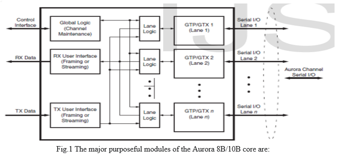
- Lane Logic: Every GTP/GTX transceiver is driven by AN instance of the lane logic module, that initializes every individual GTP/GTX transceiver and handles the coding and coding of management characters and error detection.
- World Logic: The worldwide logic module in every Aurora 8B/10B core performs the bonding and verification phases of channel low-level formatting. whereas the channel is working, the module generates the random idle characters needed by the Aurora protocol and monitors all the lane logic modules for errors.
- RX Interface: The RX user interface moves knowledge from the channel to the applying. Frames area unit conferred employing a commonplace native Link interface.
- TX user Interface: The TX user interface moves data from the application to the channel. A standard Local Link interface is used for data frames. The module has an interface for controlling clock Compensation (the periodic transmission of special characters to prevent errors due to small clock frequency Differences between connected Aurora 8B/10B cores). The Aurora 8B/10B protocol uses a symbol-based method. The minimum unit of information that is transferred across an Aurora 8B/10B channel is two symbols, called a symbol-pair. The information on an Aurora 8B/10B channel (or lane) always comprises multiple symbol-pairs. Implementations of the Aurora 8B/10B protocol accept a stream of octets from user applications and transfer them across the Aurora 8B/10B channel as one or more streams of symbol-pairs.
Transmission of user PDUs requires the following procedures:
a. Padding
b. Encapsulation with channel PDU delimiters
c. 8B/10B encoding of channel PDU payload
d. Serialization and clock encoding. Reception of user PDUs involves the following procedures:
e. Deserialization • 8B/10B decoding of channel PDU payload
f. Link layer stripping
B. Pad Stripping
The Aurora 8B/10B core is a lightweight, serial communications protocol for multi-gigabit links. It is used to transfer data between devices using one or many GTP/GTX transceivers. Connections can be full-duplex (data in both directions) or simplex. Aurora 8B/10B cores automatically initialize a channel when they are connected to an Aurora channel partner. After initialization, applications can pass data freely across the channel as frames or streams of data. Whenever data is not being transmitted, idles are transmitted to keep the link alive. Aurora frames can be any size, and can be interrupted at any time. Gaps between valid data bytes are automatically filled with idle to maintain lock and prevent excessive electromagnetic interference. The Aurora 8B/10B core detects single-bit, and most multi bit errors using 8B/10B coding rules. Excessive bit errors, disconnections, or equipment failures cause the core to reset and attempt to reinitialize a new channel.
IV. BLOCK DIAGRAM
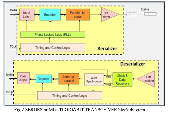
V. WORKING PRINCIPLE
- In the transmitter side the input data is given to the input latch in the continuous form. Clock signal is given to timing and control logic circuit which is connected to phase locked loop circuit.
- The PLL circuit is used to increase the frequency of the clock signal.
- From the input latch the data is transmitted to the encoder which is used to convert 8b data to 10b to maintain the dc balance and reduce bit error.
- The data is given to the parallel to serial converter from the encoder which converts the parallel data into serial data.
- The output is collected through the differential driver and then it is connected to the receiver side through the cable.
- At the receiver side the data is received through differential driver and the data is transmitted to the clock and recovery circuit in which the data is separated from the clock signal and then transmitted to word synchronizer.
- The clock signal from the word synchronizer is given to timing and control logic which is also connected to serial to parallel converter and the receiver clock signal is received.
- Then the data is given to the decoder which decodes the encoded data and transmits the data to output latch and the data is received from the output latch.
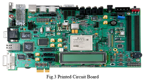
VI. PRINTED CIRCUIT BOARD
VII. ADVANTAGES
It reduces the cost of interface as it uses less number of wires.
- It supports long distance data communication.
- It is easy to implement.
- It reduces skew problem.
- It requires a smaller number of pins.
- Less number of errors.
VIII. APPLICATIONS
- Chip to chip communication
- Board to board communication
- Backplane links
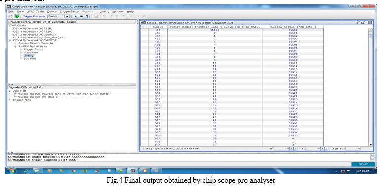
IX. RESULT
The following are the results obtained during the transmission of parallel data as well as reception and finally integrated in the chip scope pro analyser.
References
[1] Clive MAX Maxfield, “The design warriors’ guide to FPGAs”, 2004. [2] Volnei A. Pedroni, “Circuit Design with VHDL”, 2004. [3] Abhijit Atha vale and Carl Christensen of Xilinx “High speed serial I/O made simple- A designers’ guide with FPGA applications”, 2005. [4] Xilinx, Aurora 8b/10b protocol specification, available at “http://www.xilinx.com/support/documentation/ip_documentat ion/aurora_8b10b_protocol_spec_sp002.pdf”, SP002 (v2.2) April 19, 2010. [5] Xilinx, LogiCORE IP Aurora 64B/66B v6.2, available at “http://www.xilinx.com/support/documentation/ip_documentat ion/aurora_64b66b/v6_2/ds815_aurora_64b66b.pdf”, DS815 Jan, 2012. [6] Xilinx, Chip Scope Pro Software and Cores User Guide, available at “http://www.xilinx.com/support/documentation/sw_manuals/xi linx13_1/chipscope_pro_sw_cores_ug029.pdf”, UG029 (v13.1), March 1, 2011. [7] Xilinx, ISim User Guide user guide, available at “http://www.xilinx.com/support/ documentation/sw_manuals/xilinx13_1/plugin_ism.pdf”, UG660 (v 13.1) March 18, 2011. [8] Xilinx, LogiCORE Ip aurora 8b/10 v6.2 user guide, available at “http://www.xilinx.com/support/documentation/ip_documentat ion/aurora_8b10b_ug353.pdf”, UG353 (v6.2) July 23, 2010. [9] Xilinx, LogiCORE IP FIFO Generator v8.1, DS 317, 2011, available at “http://www.xilinx.com/support/documentation/ip_documentat ion/fifo_generator_ds317.pdf”, DS317 March 1, 2011.
Copyright
Copyright © 2022 A. Achyuth Kumar, Dinesh Biradar, Shiva Teja, M. Vijay Babu. This is an open access article distributed under the Creative Commons Attribution License, which permits unrestricted use, distribution, and reproduction in any medium, provided the original work is properly cited.

Download Paper
Paper Id : IJRASET43224
Publish Date : 2022-05-24
ISSN : 2321-9653
Publisher Name : IJRASET
DOI Link : Click Here
 Submit Paper Online