

Ijraset Journal For Research in Applied Science and Engineering Technology
Simulation of Junctionless Transistor for Low Power Mix Circuit
Authors: Niraj Morankar, Raj Patil, Yash Mahajan, Pranjal Patil, Santosh Wagaj
DOI Link: https://doi.org/10.22214/ijraset.2022.43253
Certificate: View Certificate
Abstract
In this work simulation of Double Gate Junction less transistor has been carried out. Comparitive study of the various parameters namely; transconductance(gm), output conductance(gd), DIBL, Subthreshold slope, Ion/Ioff, electric field and Potential. Simulation is carried out in Cogenda Visual TCAD simulator. Comparative study shows using double gate junctionless transistor reduces short channel effect such as DIBL, Subthreshold Slope, Ion/Ioff. Double Gate Junctionless transistor has higher transconductance(gm) and lower output transconductance(gd) compared to conventional junction transistor.
Introduction
I. INTRODUCTION
In order to increase the opertaing speed of circuit, improve the number of transistor on chips and reduce the manufacturing cost of chips, the size of transistors has been reducing over the time[1]. As we reduce the size of the transistor it degrades the performance of transistor due to short channel effect[3]. One of the solution of the issue could be to propose source-channel and Drain-channel junction free transistor called as junctionless transistor(JLT)[2]. Junctionless transistor has uniform doping concentration over source-channel-drain region[5].
In this project Junctionless transistor has double gates to provides better controllability of the gate voltage over drain current[4]. Junctionless and Junction Transistors are simulated in Cogenda Visual TCAD. Various analog parameters are compared between junction and junctionless transistors[6].
II. PROPOSED STRUCTURE
The proposed structure of Double Gate Junctionless Transistor is as shown in Fig.1.
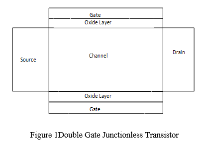
Fig.1 shows the structure of n-channel DGJLT. An n channel DGJLT has a uniform doping of N type material across source, channel and drain. Gate material used is P+ polysilicon. Length and Width of Gates is 20nm and 2nm respectively. Thickness of SiO2 layer is 1nm. Two different metal gates are used in DGJLT.Both the Gate are Interconnected. For DGJLT device, work function of both gate material are set to be 5.1eV Channel thickness of DGJLT is 10nm. Channel doping concentration (ND) across Source, Channel and Drain is 0.4*10^17 /cm^3. Thickness of SiO2 layer is 1nm.
Table 1: Device parameters
|
Parameter |
DGJLT value |
DGJT value |
|
Channel Length Channel Width |
40 nm 10 nm |
40 nm 10 nm |
|
Channel doping density Source doping density Drain doping density
|
4 x 10 ^ 17 / cm^3 -
- |
1 x 10 ^ 16 / cm^3
1 x 10 ^ 19 / cm^3 1 x 10 ^ 19 / cm^3 |
|
SiO2 layer thickness |
1 nm |
1 nm |
|
Gate m1 affinity |
5.1 eV |
5.1 eV |
|
Gate m2 affinity |
5.1 eV |
|
III. RESULTS AND DISCUSSION
Simulator Cogenda ‘VisualTCAD’ is used for analyzing device performance in various conditions. Gate work function is kept at 5.1 eV.Transfer characteristic of device for VD of 1V is shown in Fig. 2.Shows Transfer characteristics between ID and VDS for both DGJLT at Gate length from 20nm to 50nm.
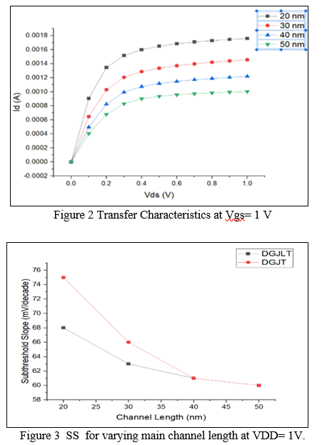
Figure 3 shows the SS of Junctionless Transistor and Junction Transistor at various channel length. SS is calculated as the slope of Id verses Vgs curve in log scale per decade i.e variation in the gate voltage required to have a decade variation in drain current. SS shows the switching characteristics of the device, lower SS has faster switching. It is observed that Junctionless Transistor has lower SS than Junction Transistor. At Channel Length 50 nm SS limits to its minimum value of 62 mV/decade. This is near to its theoretical limits of 60 mv/decade.
|
Type |
Channel Length (nm) |
SS (mV/decade) |
|
DGJT |
20 |
75 |
|
30 |
66 |
|
|
40 |
61 |
|
|
50 |
60 |
|
|
DGJLT |
20 |
68 |
|
30 |
63 |
|
|
40 |
61 |
|
|
50 |
60 |
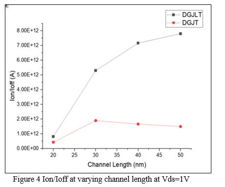
Figure 4 shows the Ion/Ioff of Junctionless Transistor and Junction Transistor at various channel length. To get the value of Ion, Vgs is kept at 1V and apply 1 V to Vd, whereas to find out Ioff value of Vgs is set to 0 V and Vd is set to 1V. . It is observed that Junctionless Transistor has higher Ion/Ioff ratio than Junction Transistor.
|
Type |
Channel Length (nm) |
Ion/Ioff (A) |
|
DGJT |
20 |
4.36E11 |
|
30 |
2.46E11 |
|
|
40 |
1.66E11 |
|
|
50 |
1.49E11 |
|
|
DGJLT |
20 |
8.13E11 |
|
30 |
5.29E12 |
|
|
40 |
7.16E12 |
|
|
50 |
7.79E12 |
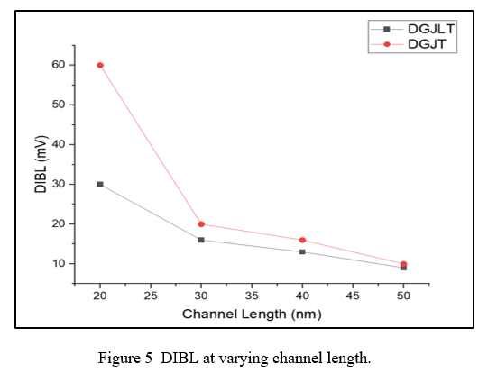
Figure 5 shows the DIBL of the DGJLT and DGJT at with various channel length. DIBL can be calculated as difference in threshold voltage for drain voltage at 50mV and 1V. It is observed that DIBL in case of Junctionless Transistor is lower than Junction Transistor for all channel length. As channel length shrink the DIBL increases. For the Junctionless Transistor value of DIBL is approximately half than Junction Transistor.
|
Type |
Channel Length (nm) |
DIBL (mV) |
|
DGJT |
20 |
60 |
|
30 |
20 |
|
|
40 |
16 |
|
|
50 |
10 |
|
|
DGJLT |
20 |
30 |
|
30 |
16 |
|
|
40 |
13 |
|
|
50 |
9 |
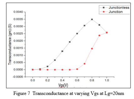
Figure 7 shows the Transconductance(gm) of proposed Junctionless Transistor and Junction Transistor, at Vds = 1 V and Channel length of 20 nm. Transconductance (gm) is ratio of change in Drain Current(Id) to the change in Gate Voltage(Vgs) at constant Drain to Source voltage(Vds) (gm= δId/δVgs). For better performance of any device Transconductance(gm) of the device is must high. It can be observed that the Double Gate Junctionless Transistor has higher Transconductance in than Junction Transistor.
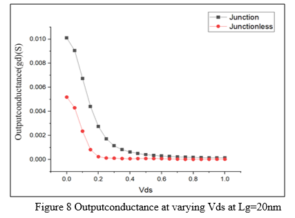
Figure 8 shows the Output Conductance(gd) of Junctionless Transistor and Junction Transistor, at Vgs = 1V and Lg= 20 nm. Output Conductance(gd) is ratio of change in Drain Current (Id) to change in Drain to Source Voltage (Vds) by keeping Gate Voltage(Vgs) constant (gd = δId / δVds). Output Conductance reciprocal of output resistance (Ro). Therefore, for good device performance Output Conductance(gd) of the device should be low. . It can be observed that the Double Gate Junctionless Transistor has lower Output Conductance in than Junction Transistor.
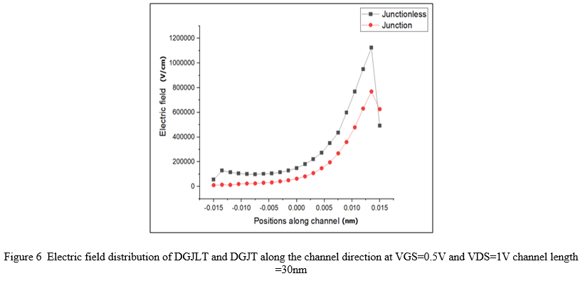
Figure 6 shows the electric field distribution along the channel length at Vgs=0.5V and Vds=1V and channel length of 30 nm. It Is observed that junctionless transistor has higher electric field compared junction transistor. Both Transistors have higher electric field near drain side of channel.
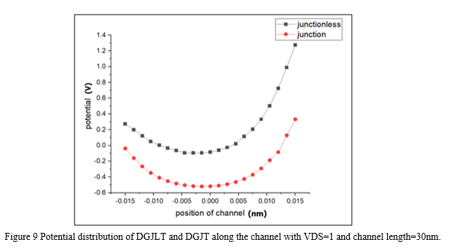
Figure 9 shows the potential distribution along the channel length. At Drain voltage(Vds)=1V and gate voltage(Vgs) of 0V to 1V and channel length is 30 nm. It is observed that junctionless transistor has higher potential along the channel compared to junction transistor.
Conclusion
All the device parameters are simulated in 2D environment with Cogenda VisualTCAD. It is Observed that when channel length is lesser i.e 20 nm, Junctionless transistor has better results for DIBL (50% improvement). It has better short channel performance in terms of Ion/Ioff ratio and subthreshold slope. Surface potential and Electric Field under channel is improved. Analog Parameters of device is also improved in terms of higher transconductance and lower output conductance. Thus DGJLT is a better device for CMOS technology.
References
[1] G. V. Reddy and M. J. Kumar, \"A new dual-material double-gate (DMDG) nanoscale SOI MOSFET-two-dimensional analytical modeling and simulation,\" in IEEE Transactions on Nanotechnology, vol. 4, no. 2, pp. 260-268, March 2005, doi: 10.1109/TNANO.2004.837845. [2] J. Singh, V. Gadi and M. J. Kumar, \"Modeling a Dual-Material-Gate Junctionless FET Under Full and Partial Depletion Conditions Using Finite-Differentiation Method,\" in IEEE Transactions on Electron Devices, vol. 63, no. 6, pp. 2282-2287, June 2016, doi: 10.1109/TED.2016.2555082. [3] R. Trevisoli, R. T. Doria, M. de Souza, S. Barraud, M. Vinet and M. A. Pavanello, \"Analytical Model for the Dynamic Behavior of Triple-Gate Junctionless Nanowire Transistors,\" in IEEE Transactions on Electron Devices, vol. 63, no. 2, pp. 856-863, Feb. 2016, doi: 10.1109/TED.2015.2507571. [4] J. P. Colinge et al., \"SOI gated resistor: CMOS without junctions,\" 2009 IEEE International SOI Conference, 2009, pp. 1-2, doi: 10.1109/SOI.2009.5318737. [5] I. Wong, Y. Chen, S. Huang, W. Tu, Y. Chen and C. W. Liu, \"Junctionless Gate-All-Around pFETs Using In-situ Boron-Doped Ge Channel on Si,\" in IEEE Transactions on Nanotechnology, vol. 14, no. 5, pp. 878-882, Sept. 2015, doi: 10.1109/TNANO.2015.2456182. [6] H. Lou et al., \"A Junctionless Nanowire Transistor With a Dual-Material Gate,\" in IEEE Transactions on Electron Devices, vol. 59, no. 7, pp. 1829-1836, July 2012, doi: 10.1109/TED.2012.2192499.
Copyright
Copyright © 2022 Niraj Morankar, Raj Patil, Yash Mahajan, Pranjal Patil, Santosh Wagaj. This is an open access article distributed under the Creative Commons Attribution License, which permits unrestricted use, distribution, and reproduction in any medium, provided the original work is properly cited.

Download Paper
Paper Id : IJRASET43253
Publish Date : 2022-05-25
ISSN : 2321-9653
Publisher Name : IJRASET
DOI Link : Click Here
 Submit Paper Online