

Ijraset Journal For Research in Applied Science and Engineering Technology
DC Booster with Voltage Multiplier for Renewable Energy Sources
Authors: Rashmi R, T. Senthil Kumar
DOI Link: https://doi.org/10.22214/ijraset.2022.42821
Certificate: View Certificate
Abstract
An high step-up interleaved dc-dc converter is proposed for high efficiency and voltage gain applications. The configuration is proposed of modified two-phase interleaved boost converter with parallel-input series-output connections and a voltage multiplier module stacking on the output side. In the proposed converter, the parallel-input connection is used to share the input current and to reduce the conduction losses, while the series-output connection and voltage multiplier module are deployed to obtain the high voltage gain without operating at maximum duty ratio. In addition, the input current ripple is reduced due to the interleaved operation. The voltage stresses on the power switches are extremely lower than the output voltage such that the low-voltage-rated MOSFETs with low conduction resistor are available to reduce the conduction losses and to improve the conversion efficiency. Meanwhile, the output diode reverse-recovery problem is alleviated by the leakage inductance of the coupled inductors. Finally, the experimental results from a 1-kW prototype are given to validate the effectiveness of the proposed converter.
Introduction
I. INTRODUCTION
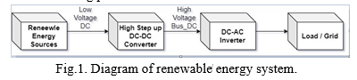
In renewable energy systems, such as photovoltaic (PV) and fuel cell generation systems, high voltage-gain and high- efficiency of dc-dc converters play a major role as a medium between the low output voltages of these sources and the utility grid. If the line voltage is at 220 Vac, a 380-400V dc voltage bus is needed for the inverter. However, the output voltages of PV and fuel cells are actually ranged from 24 to 40 V due to the safety and reliability considerations. Thus, a dc-dc converter with a high voltage gain is required to boost the outputs of PV and fuel cells.
In general, a conventional boost converter can be deployed to provide a high voltage gain with a maximum duty ratio. However, it leads to large current ripple, high switching losses, severe output diode reverse- recovery problem and electromagnetic interference (EMI) problem. Moreover, the voltage stresses on the power switch and the output diode are equal to the output voltage, the high-voltage-rated MOSEFTs with large conduction resistance are necessary in the high output- voltage conversion system, which leads to large conduction and switching losses. These problems are the main limitations for the conventional boost converter. Commonly, the interleaved boost converter structure is deployed in high current applications to reduce/minimize the current ripple, reduce the size of the magnetic elements and increase the power level due to its advantages of current ripple cancellation and current-sharing performance.
In order to obtain high step-up voltage gain and high efficiency, many converter topologies have been proposed in the literature. Coupled inductor-based converters are good options for high voltage gain by changing the turns ratio of the coupled inductor. However, the leakage inductance of the coupled inductor causes power loss and high voltage stress on the power switches. The switched-capacitor converter can also achieve high voltage gain conversion. However, these converters require much number of switches, which leads to the complexity of the driving circuit. Some kinds of interleaved high step-up converter with voltage multiplier cells which consist of diodes and capacitors have been proposed. There are some advantages in these converters, such as lower voltage stresses on the switches and diodes, reduction of the input current ripple and high voltage conversion ratio without maximum large duty ratio.
An interleaved high step-up DC-DC converter with high voltage gain and high efficiency is proposed in this paper, which is eligible for power conversion in the renewable energy systems as shown in Fig.1. The proposed converter configuration is composed of modified two-phase interleaved boost converter with parallel-input series-output connection and a voltage multiplier module to achieve higher voltage gain as shown in Fig. 2. The voltage multiplier module is realized by the secondary windings of two coupled inductors and two switched capacitor. The power switches are driven in the interleaved fashion with half switching period shift. The advantages of the proposed converter are as follows.
- The proposed converter achieves high voltage gain without operating at extreme duty ratio.
- The voltage stress on the power switches are greatly lower than the output voltage such that the low-voltage-rated MOSFETs with low conduction resistances can be used to reduce the conduction losses.
- The parallel-input architecture can share the input current, reduce the conduction losses and handle large input current applications.
- The input current ripple is decreased by the interleaved operation of the proposed converter, which can enlarge the lifetime of renewable energy sources.
- The reverse-recovery problem of output diodes are alleviated due to the leakage inductances of the coupled inductors. The leakage energy of the coupled inductors is recycled such that the voltage spikes on the power switches are avoided and the efficiency is improved.
All these features show that the proposed converter is suitable for high voltage gain, high efficiency and high power applications. The experimental results on a 1-kW prototype circuit are provided to validate the performance of the proposed converter.
II. CONVERTER CONFIGURATION AND OPERATIONAL PRINCIPLE ANALYSIS
A. Converter Configuration
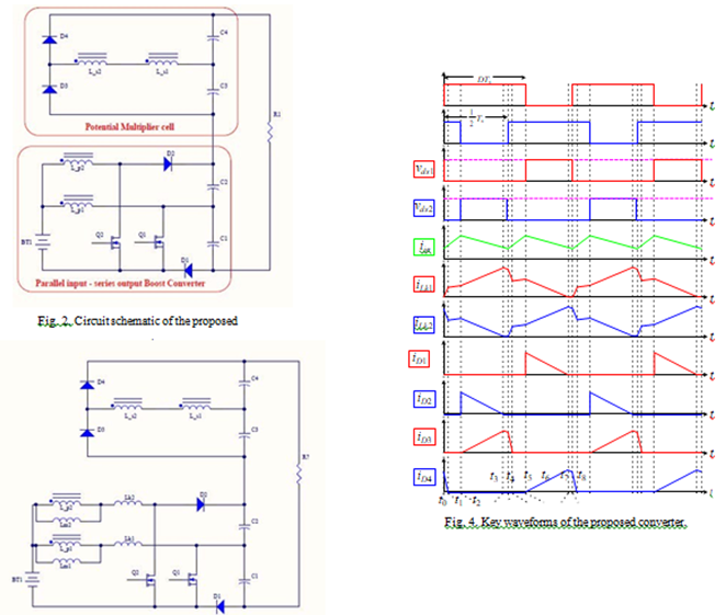
The proposed interleaved high step-up converter is shown in Fig.2. The configuration is composed of modified two- phase interleaved boost converter with parallel-input series- output connection and a voltage multiplier module stacking on the output side to achieve higher voltage gain. There are two coupled inductors in the proposed converter. The coupling references of the coupled inductors are denoted by the marks “? ” and “ ? ” as given in Fig. 2. The coupled inductor is modeled as a combination of an ideal transformer with a turns ratio n, a magnetizing inductance and leakage inductance in this paper. The voltage multiplier module is realized by the secondary windings of two coupled inductors, two output diodes D3 and D4 and two switched capacitors C3 and C4 .
The equivalent circuit of the proposed converter is shown in Fig. 3, where Lm1 and Lm2 are the magnetizing inductances, Lk1 and Lk 2 are the leakage inductances, n is defined as the turns ratio Ns / Np . S1 and S2 are the power switches. C1 and C2 are the output capacitors. D1 and D2 are the output diodes. The power switches S1 and S2 work in the interleaved mode with 180? phase shift and the same duty ratio. The duty ratio is greater than 0.5. The key waveforms are depicted in Fig. 4 when the proposed converter is operated in the steady-state and continuous conduction mode (CCM).
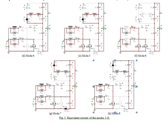
Under the steady-state operation of the proposed converter, there are eight operational modes in a switching period. The equivalent circuits for each mode are shown in Fig. 5.
- Mode 1 [ t0 ? t1 ]: At t ? t0 , S1 begins to turn on with zero-current condition, while S2 remains in the turn-on state. The diodes D1, D2 and D3 are reverse-biased, as shown in Fig. 5(a). iLk1 increases quickly and its rate of increment is Fig. 5(a). iLk1 increases quickly and its rate of increment is transfers to the secondary side of coupled inductors charging C4 via D4 when iLk1 ? iLm1. The current through the diode D4 decreases and its falling rate is controlled by Lk1 and Lk 2 , which alleviates the diode reverse recovery problem of D4 . This mode ends when iD4 decreases to zero and D4 turns off.
- Mode 2 [ t1 ? t2 ]: At t ? t1 , S1 and S2 are in the turn-on state. All diodes are reverse-biased, as shown in Fig. 5(b). The magnetizing inductors Lm1 and Lm2 as well as leakage inductances Lk1 and Lk 2 are linearly charged by Vin. The voltage stress on D1 and D2 is the voltage on C1 and C2 , respectively. This mode ends when S2 is turned off.
- Mode 3 [ t2- t3 ]: At t = t2 , S2 is turned off, which makes the diodes D2 and D3 turn on, as shown in Fig. 5(c). The energy stored in the magnetizing inductor Lm2 is transferred to the secondary side of coupled inductors charging C3 via D3, meanwhile iLk 2 flows through D2 , C2 and S1 , so that C2 is charged. The voltage stress on S2 is clamped by VC 2. iLk 2 decreases to alleviate the reverse recovery problem for D2 . Vin , Lm2 and Lk 2 release energy to the output side. This mode ends at t3 , when iLk 2 decreases to zero and D2 turns off.
- Mode 4 t3 ? t4 ]: At t ? t3 , iLk 2 decreases to zero and the diode D2 turns off, as shown in Fig. 5(d). Thus, there is no diode reverse recovery losses for D2 . The energy stored in Lm2 is still transferred to the secondary side of coupled inductors. The current through S1 is equal to the summation of iLm1 and iLm2. This mode ends when S is turned on.
- Mode 5 [ t4 - t5 ]: At t = t4 , S2 is turned on with ZCS due to the leakage inductor L , while S remains in the turn-on state. The diodes D1, D2 and D4 are reverse-biased, as shown in Fig. 5(e). iLk2 increases with high rate. The energy stored in Lm2 still transfers to the secondary side of coupled inductors charging C3 via D3 when iLk2 ? iLm2 .iD3 decreases and its current falling rate is controlled by Lk1 and Lk 2 , which alleviates the diode reverse recovery problem for D3 . This mode ends when iD3 decreases to zero and D3 turns off.
- Mode 6 [t5 ? t6 ]: At t ? t5 , S1 and S2 are in the turn-on state. All diodes are reverse-biased, as shown in Fig. 5(f). The magnetizing inductances Lm1 and Lm2 as well as leakage inductances Lk1 and Lk 2 are linearly charged by Vin. This mode ends when S1 is turned off.
- Mode 7 [ t6 ? t7 ]: At t ? t6 , S1 is turned off, which makes D1 and D2 turn on, as shown in Fig. 5(g). The energy stored in Lm1 begins to transfer to the secondary side of coupled inductors charging C4 via D4. Meanwhile iLk1 decreases and flows through C1 and D1. This mode ends at t7 , when iLk1 decreases to zero and the diode D1 turns off.
- Mode 8 [ t7 - t8 ]: At t = t7 , the diode D1 turns off with zero-current condition, as shown in Fig. 5(h). There is no diode reverse recovery losses for diode D1. The energy stored in Lm1 is still transferred to the secondary side of coupled inductors. The current through S2 is equal to the summation of iLm1 and iLm2. This mode ends when the switch S1 is turned on. The next switching period subsequently begins.
III. STEADY-STATE ANALYSIS
To simplify the steady-state analysis of the proposed converter in CCM, some assumptions are made as follows. The capacitances are sufficiently large, such that the voltages on the capacitors are considered as constant in one switching period. Two coupled inductors are considered to be identical, namely Ns1 /N p1 = Ns 2/N p 2 = n , Lm1 = Lm2 = Lm , Lk1 = Lk 2 = Lk , and the coupling coefficient k = Lm/(Lm + Lk ) .
A. Voltage Conversion Ratio
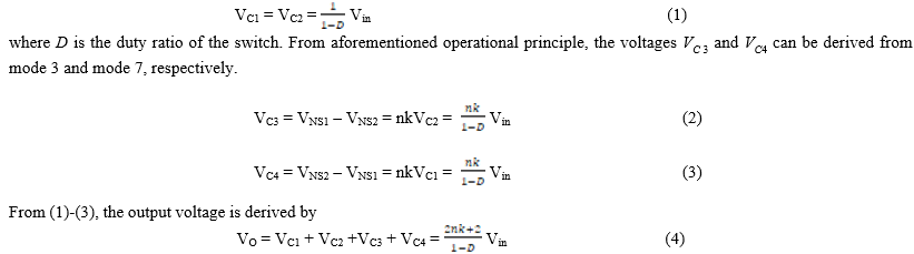
The voltages on the capacitors C1 and C2 can be calculated analogously to conventional boost converter, which are given by
IV. EXPERIMENTAL RESULTS
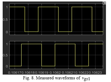
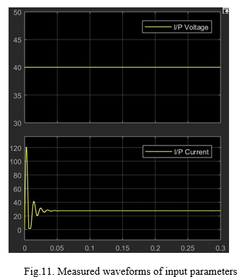
In order to verify the effectiveness of the proposed converter, a 1000-W prototype with 40-V input voltage, 400- V output voltage and the switching frequency 40 kHz is built and tested with the parameters as follows.
Lm1 , Lm 2 : 135 µH ; Lk1 , Lk 2 : 1 µH ; C1 ,C2 ,C3 ,C4 : 100 µF ; D1 , D2 , D3 , D4 : DSEC60-03A; S1 , S2 : IRFP4227; n ? 1 .
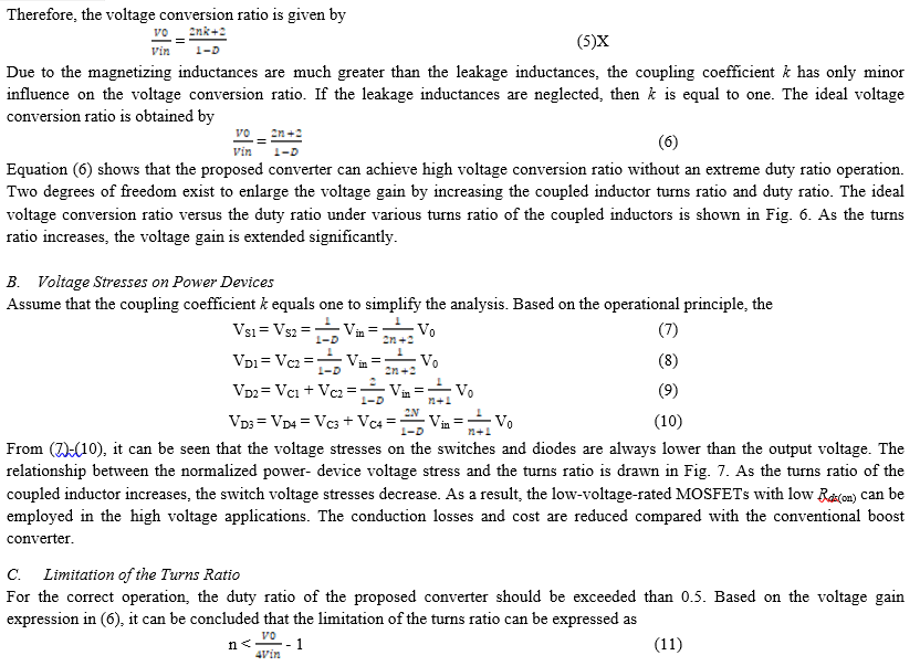
The following experimental results from Figs. 8-11 are given under 1000-W full-load condition.
The measured waveforms of the gate signals vgs1 and vgs 2, and the drain-source voltages vds1 and vds 2 are shown in Fig. 8. The extreme duty ratio existed in the conventional interleaved boost converter is avoided because the voltage gain of the proposed converter is extended. The switch voltage stress is about 100 V, which is only one-fourth of the output voltage. Therefore, low-voltage-rated MOSFETs with low Rds(on) are available to reduce the conduction losses.
Fig. 9 shows the measured waveforms of the input current iin and the leakage inductance currents iLk1 and iLk2 with iin = iLk1 + iLk2. It can be seen that the input current ripple of im is much lower than those of iLk1 and iLk2 due to the interleaved operation.
The voltage and current waveforms on the diodes D1 ~ D4 are given in Fig. 10 and Fig. 11. It is shown that there is almost no reverse recovery current because the diode turn- off current is controlled by the leakage inductances of the coupled inductors. As a result, the reverse recovery losses are minimized and the EMI noise is suppressed compared with the conventional interleaved boost converter. Furthermore, the voltage stress on the diode D1 is about 100V and that on the diodes D2 ~ D4 is 200V, which is consistent with the results of steady-state analysis and lower than the high output voltage.
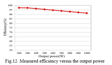
Fig. 12 shows the experimental conversion efficiency at different loads measured by the power analyzer (HIOKI 3390). The maximum efficiency is around 97.44% at Po = 200 W. The full-load efficiency is appropriately 91.39%. The results show the proposed converter has high-efficiency conversion.
Conclusion
An interleaved high step-up DC-DC converter with parallel-input and series-output configuration and voltage multiplier module is proposed in this paper. The voltage conversion ratio can be greatly extended and the extreme duty ratio can be avoided in the high voltage gain applications. The switch voltage stress is much lower than the output voltage. As a result, low-voltage-rated MOSFETs with low on-resistance can be adopted to reduce the conduction losses. The input current ripple is reduced by the interleaved operation. The output diode reverse-recovery problem is alleviated by the leakage inductances of the coupled inductors to reduce reverse-recovery losses. Finally, a 1-kW prototype of the proposed converter is built to show the converter performance. The experimental results have demonstrated the proposed converter is suitable for the high voltage- gain and high efficiency applications.
References
[1] B. Yang, W. Li, Y. Zhao, and X. He, “Design and analysis of a grid connected PV power system,” IEEE Trans. Power Electron., vol. 25, no. 4, pp. 992–1000, 2010. [2] J. M. Carrasco, L. G. Franquelo, J. T. Bialasiewicz, E. Galvan, et. al., “Power-electronic systems for the grid integration of renewable energy sources: A survey,” IEEE Trans. Ind. Electron., vol. 53, no. 4, pp. 1002–1016, 2006. [3] A. Ajami, H. Ardi, and A. Farakhor, “A novel high step-up DC-DC converter based on integrating coupled inductor and switched-capacitor techniques for renewable energy applications,” IEEE Trans. Power Electron., vol. 30, no. 8, pp. 4255–4263, 2015. [4] F. L. Tofoli, D. C. Pereira, W. J. Paula and D. S. O. Junior, “Survey on non-isolated high-voltage step-up DC–DC topologies based on the boost converter,” IET Power Electron., vol. 8, no. 8, 2044–2057, 2015. [5] R. W. Erickson and D. Maksimovic, Fundamentals of Power Electronics, 2nd ed. Norwell, MA, USA: Kluwer, 2001. [6] Y. P. Hsieh, J. F. Chen, T. J. Liang, and L. S. Yang, “Novel high step- up DC–DC converter with coupled-inductor and switched-capacitor techniques,” IEEE Trans. Industrial Electronics, vol. 59, no. 2, pp. 998–1007, 2012. [7] X. Hu, and C. Gong, “A high voltage gain DC-DC converter integrating coupled-inductor and diode-capacitor techniques,” IEEE Trans. Power Electron., vol. 29, no. 2, pp. 789–800, 2014. [8] T. F. Wu, Y. S. Lai, J. C. Hung, and Y. M. Chen, “Boost converter with coupled inductors and buck–boost type of active clamp,” IEEE Trans. Ind. Electron., vol. 55, no. 1, pp. 154–162, 2008. [9] R. J.Wai and R. Y. Duan, “High step-up converter with coupled- inductor,” IEEE Trans. Power Electron., vol. 20, no. 5, pp. 1025–1035, 2005. [10] C. L. Wei, and M. H. Shih, “Design of a switched -capacitor DC-DC converter with a wide input voltage range,” IEEE Trans. Circuits and Systems, Vol. 60, No. 6, pp. 1648–1656, 2013. [11] H. S. Chung, A. Ioinovici, and W. L. Cheung, “Generalized structure of bi-directional switched-capacitor dc/dc converters,” IEEE Trans. Circuits Sys. I,Regul. Pap., vol. 50, no. 6, pp. 743–753, 2003. [12] K. C. Tseng, and C. C. Huang, “High step-up high-efficiency interleaved converter with voltage multiplier module for renewable energy system,” IEEE Trans. Ind. Electron., vol. 61, no. 3, pp. 1311– 1319, 2014. [13] X. Hu and C. Gong, “A high gain input-parallel output-series DC/DC converter with dual coupled inductors,” IEEE Trans. Power Electron., vol. 30, no. 3, pp.1306–1327, 2015. [14] W. Li, Y. Zhao, J. Wu, and X. He, “Interleaved high step-up converter with winding cross coupled inductors and voltage multiplier cells,” IEEE Trans. Power Electron., vol. 27, no. 1, pp. 133–143, 2012.
Copyright
Copyright © 2022 Rashmi R, T. Senthil Kumar. This is an open access article distributed under the Creative Commons Attribution License, which permits unrestricted use, distribution, and reproduction in any medium, provided the original work is properly cited.

Download Paper
Paper Id : IJRASET42821
Publish Date : 2022-05-17
ISSN : 2321-9653
Publisher Name : IJRASET
DOI Link : Click Here
 Submit Paper Online