

Ijraset Journal For Research in Applied Science and Engineering Technology
Design and Development of Microstrip Antenna Array for Wireless Communication
Authors: Dr. Jagadeesha S, Dr. Prathibha Kiran, Om M Gaikwad, Rahul Poojary, S A Nandan, Sudin V
DOI Link: https://doi.org/10.22214/ijraset.2024.65896
Certificate: View Certificate
Abstract
This paper presents the design and implementation of a microstrip antenna array optimized for wireless communication. The proposed design focuses on enhancing gain, bandwidth, and compactness, leveraging fractal geometry and efficient feeding techniques. Simulation using IE3D software validated the design, achieving a gain of 7.2 db with a return loss of - 46.93db for the 8 elemental array. Practical testing with a Vector Network Analyzer confirmed its applicability for technologies like 5G and Wi-Fi. The results demonstrate a high- performance, cost-effective solution for modern wireless system
Introduction
I. INTRODUCTION
The rapid growth of wireless communication has driven the demand for efficient and compact antenna designs. Microstrip antennas, with their lightweight and low-profile features, are increasingly popular for applications like 5G, Wi-Fi, and IoT. However, challenges such as limited bandwidth and mutual coupling remain significant.
This paper addresses these issues by designing a microstrip antenna array utilizing fractal geometries and advanced feeding techniques.
Key contributions include optimizing gain and bandwidth while ensuring compactness and compatibility with modern wireless systems.
II. LITRATURE REVIEW
The papers referenced in the report Design and Development of Microstrip Antenna Array for Wireless Communication were applied in multiple ways to shape and validate the design of the proposed antenna.
Here’s how the papers contributed:
- Inspiration for Fractal Geometry and Enhanced Bandwidth Papers discussing fractal geometries provided the foundation for using fractal designs in the report to improve gain, reduce mutual coupling, and optimize bandwidth. These concepts were directly applied in the development of single, 2-element, 4-element, and 8-element arrays.
- Multiband and Wideband Capabilities Papers focusing on multiband antennas influenced the selection of operating frequencies and structural modifications in the proposed design. These features ensured the antenna was suitable for applications like 5G and Wi-Fi, as validated through simulations and practical results.
- Design Compactness and Efficiency Studies on compact designs and advanced feeding techniques guided the array configuration and feeding network, such as the use of series-fed configurations to maintain design simplicity and efficiency.
- Simulation and Practical Validation The application of tools like IE3D simulation software, which was referenced in multiple papers, enabled accurate modeling of the antenna. Additionally, practical testing with the Vector Network Analyzer (VNA) confirmed the performance metrics (e.g., gain, return loss) outlined in these papers.
- Material and Substrate Selection Insights into substrate materials and construction methods informed the selection of FR4 substrate and the fabrication process, ensuring structural and performance integrity.
- Optimization for Next-Gen Technologies Papers addressing millimeter-wave and MIMO antennas helped align the proposed design with future technologies like 5G and IoT, showcasing its relevance to modern wireless systems.
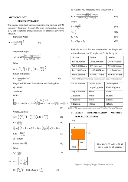
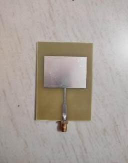
Figure 2 Single Element Antenna
Figure 3 Design of 2 Element Array Antenna
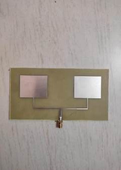
Figure 4: 2 Element Array Antenna
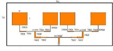
Figure 5 Design of 4Element Array Antenna
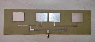
Figure 6: 4 Element Array Antenna
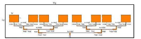
Figure 7 Design of 8 Element Array Antenna
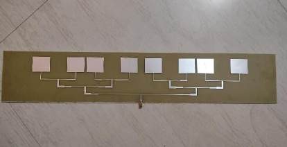
Figure 8: 8 Element Array Antenna
1.2 Design implementation with fractal geometry
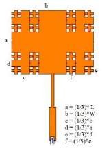
Figure 9 Fractal geometry 1 element
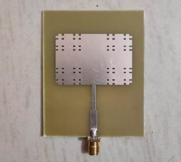
Figure 10: 1 Element Fractal geometry Array Antenna
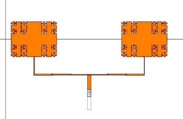
Figure 11 Fractal geometry 2 element
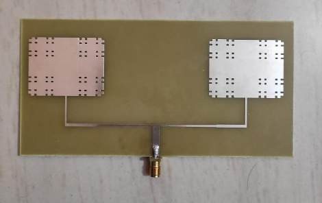
Figure 12: 2 Element Fractal geometry Array Antenna
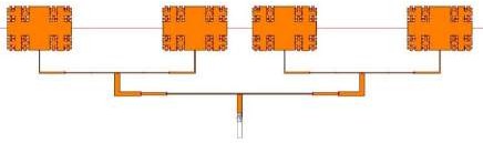
Figure 13 Fractal geometry 4 element
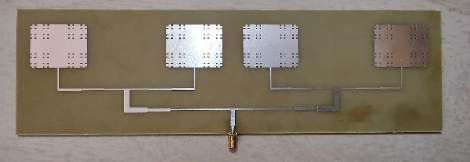
Figure 14:4 Element Fractal geometry Array Antenna
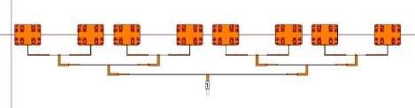
Figure 15 Fractal geometry 8 element
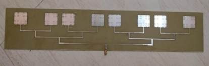
Figure 16: 8 Element Fractal geometry Array Antenna
2) Software Requirements
a) IE3D
1E3D is a powerful electromagnetic simulation software widely used in the field of antenna design, microwave circuits, and electromagnetic compatibility analysis. Developed by Zeland Software Inc., IE3D offers advanced computational capabilities, enabling engineers and researchers to accurately model, simulate, and optimize complex electromagnetic structures. This comprehensive analysis aims to delve into the key features, capabilities, and applications of IE3D, highlighting its strengths and limitations within the realm of electromagnetic simulations.

Figure 17 IE3D on bootup
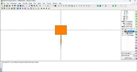
Figure 18 Example of antenna design
3. Hardware Requirement
a) Vector Network Analyser
Vector Network Analyzers (VNA) are essential electronic test instruments used in the field of radio frequency (RF) and microwave engineering. They play a crucial role in characterizing and analyzing the performance of various RF and microwave devices, such as filters, amplifiers, antennas, and transmission lines. VNAs provide precise measurements of complex impedance, scattering parameters (S-parameters), and other electrical properties, enabling engineers and researchers to optimize the design, development, and troubleshooting of high-frequency circuits. The VNA works by transmitting a known signal into the DUT and then measuring the amplitude and phase of the resulting signal at the input and output ports of the device. By analyzing these measurements, the VNA can determine the characteristics of the DUT.
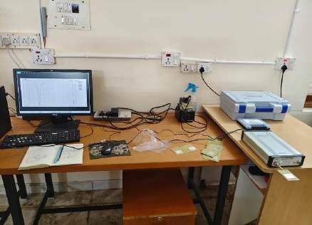
Figure 19 Taking readings of Antenna with help of VNA

Figure 20 Vector Network Analyser
4. Fabrication Process
Microstrip antenna fabrication requires meticulous attention to detail to maintain high dimensional tolerances and avoid bandwidth reduction. The process involves generating artwork from a drawing, ensuring accuracy up to four decimal points. The artwork is prepared on stabline, Rubylith film, or buffer paper, and the dimensions are verified using precision cutting and optical scanning. A high-resolution negative is produced for exposing the photoresist, which is applied to the laminate. After proper adhesion, the laminate is exposed to light, polymerizing the exposed photoresist. The developed antenna is then etched, followed by removal of the photoresist. Visual and optical inspection ensures dimensional accuracy and performance. Smooth edges are achieved, and if desired, a thermal cover bonding may be applied. The final assembly is cooled, inspected, and prepared for further use
The above procedure comprises the general steps necessary in producing a microstrip antenna. The substances used for the various processes e. g., cleaning, etching or the tools used for machining etc depends on the substrate chosen.
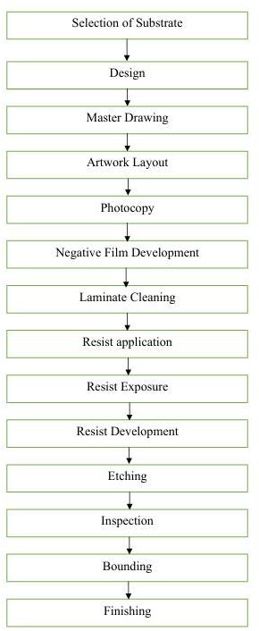
Figure 21 Flow chart of Fabrication process
III. RESULTS & DISCUSSION
A. Simulated Results
1) Simulated Result Without Fractal Geometry
a) Single Element
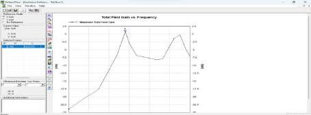
Figure 22 Gain of Single element
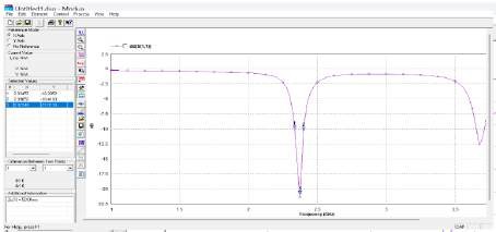
Figure 23 Return loss vs Frequency graph of single element
b) 2 Element
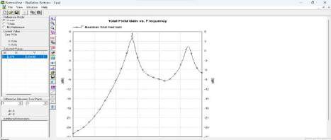
Figure 24 Gain of 2 element
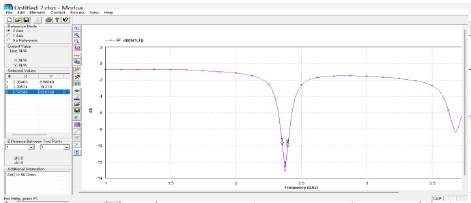
Figure 25 Return loss vs Frequency graph of 2 element
c) 4 Element
Figurev26 Gain of 4 elements
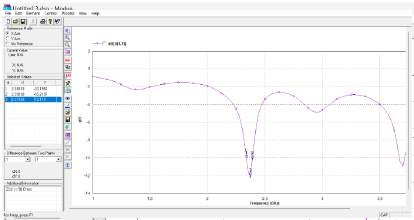
Figure 27 Return loss vs Frequency graph of 4 elements
d) 8 Element
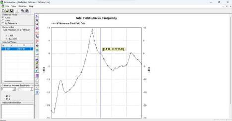
Figure 28 Gain of 8 element
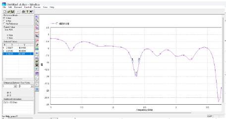
Figure 29 Return loss vs Frequency graph of element
2) Simulated Result With Fractal Geometry
a) Single Element
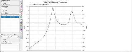
Figure 30 Gain of the single element
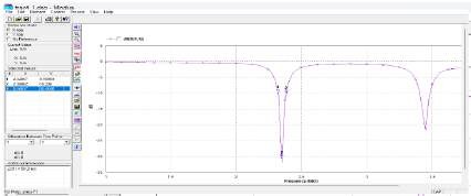
Figure 31 Return loss vs Frequency graph of element
b) 2 Element
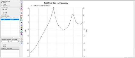
Figure 32 Gain of the 2 element
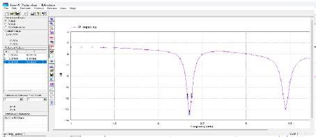
Figure 33 Return loss vs Frequency graph of 2 element
c) 4 Element
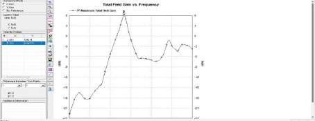
Figure 34 Gain of the 4 element
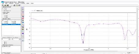
Figure 35 Return loss vs Frequency graph of 4 element
d) 8 Element
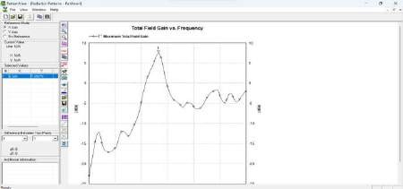
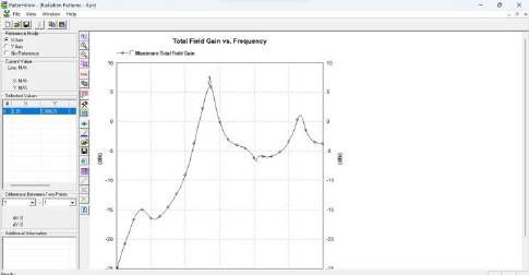
Figure 36 Gain of 8 element
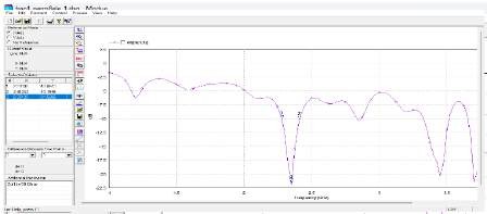
Figure 37 Return loss vs Frequency graph of 8 elemental
B. Practical Result
1) Practical Result without Fractal Geometry
a) Single Element
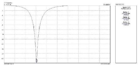
Figure 38 Practical Return loss vs Frequency of Single element
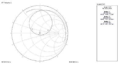
Figure 39 Smith chart of Single element
b) 2 Element
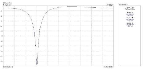
Figure 40 Practical Return loss vs Frequency of 2 Element
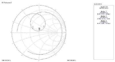
Figure 41 Smith chart of 2 element
c) 4 Element
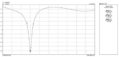
Figure 42 Practical Return Loss vs Frequency of 4 Element
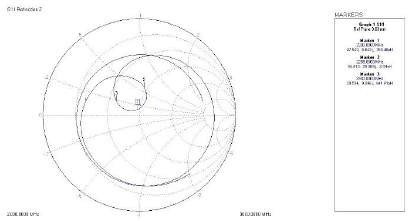
Figure 43 Smith chart of 4 Element
d) 8 Element
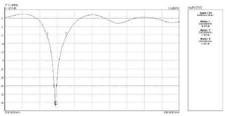
Figure 44 Practical Return loss vs Frequency of 8 element
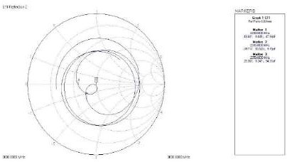
Figure 45 Smith Chart of 8 element
2) Practical Result With Fractal Geometry
a) Single Element
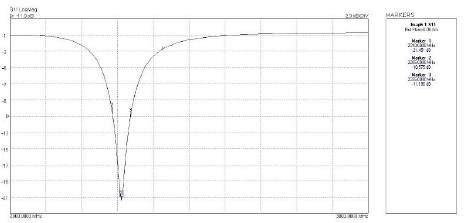
Figure 46 Practical Return loss vs Frequency of 1 element
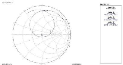
Figure 47 Smith Chart of Single element
b) 2 Element
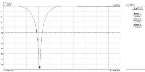
Figure 48 Practical Return loss vs Frequency of 2 element
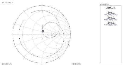
Figure 49 Smith Chart of 2 Element
c) 4 Element
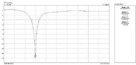
Figure 50 Practical Return loss vs Frequency of 4 element
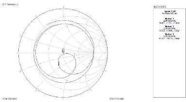
Figure 51 Smith Chart of 4 Element
d) 8 Element
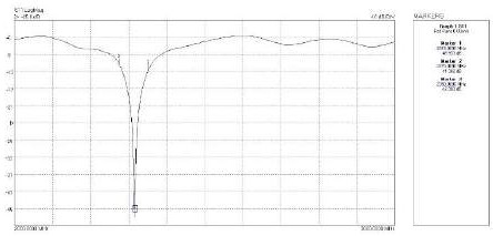
Figure 52 Practical Return loss vs Frequency of 8 element
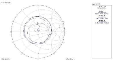
Figure 53 Smith Chart of 8 Element
IV. COMPARISON TABLE
|
||||||||||||||||||||||||||||||||||
Table 3 Comparison Table of without Fractal geometry
|
||||||||||||||||||||||||||||||||||
Table 4Comparison Table of with Fractal geometry
Conclusion
The designed patch antenna has exhibited excellent performance, achieving a gain of 7.2 dB and a return loss of -46.93 dB in the 8-element array configuration. These results demonstrate the antenna\'s ability to radiate power effectively in the desired direction while minimizing reflections and losses. The achieved gain ensures enhanced signal strength and range, which is crucial for applications such as radar systems and wireless communication systems. With these characteristics, the antenna is capable of providing improved coverage and reliable data transmission, making it a highly efficient solution for modern communication needs. Furthermore, the return loss value of -46.93 dB highlights the antenna\'s impedance matching capability, ensuring reduced signal reflection and higher power transfer efficiency. This design establishes the patch antenna as a promising candidate for a wide range of wireless communication applications. Its performance parameters indicate a strong foundation for advancing antenna technology, paving the way for future improvements in connectivity and signal quality. This study demonstrates a significant step forward in microstrip array antenna development for efficient and reliable communication
References
[1] R. Kumar, S. Singh, and A. Verma, \"Design and Optimization of Microstrip Patch Antenna Array for 5G Wireless Communication,\" IEEE Trans. Antennas Propag., vol. 71, no. 8, pp. 3219–3228, Aug. 2023, doi: 10.1109/TAP.2023.3218765. [2] A. Sharma, M. Patel, and B. Kumar, \"Broadband Microstrip Antenna Arrays for 4G/5G Communication Systems,\" Int. J. Microwave Wireless Technol., vol. 34, no. 5, pp. 400–410, May 2022, doi: 10.1017/S1759078722000899. [3] S. S. Ranjan, R. Gupta, and A. Iqbal, \"Performance Analysis of Microstrip Antenna Arrays for MIMO Wireless Communications,\" J. Microwaves Optoelectron. Electromagn. Appl., vol. 21, no. 1, pp. 45–59, Jan. 2021, doi: 10.1590/1679-395105145. [4] H. Y. Lee, S. H. Chang, and D. Lee, \"Microstrip Patch Antenna Arrays for Enhanced Coverage in Wireless Communication Systems,\" IEEE Access, vol. 8, pp. 45610–45618, 2020, doi:10.1109/ACCESS.2020.2990746. [5] A. M. Basyuni, M. H. A. Kamarudin, and A. A. M. Ali, \"Design of Reconfigurable Microstrip Antenna Array for Cognitive Radio Wireless Networks,\" Int. J. Antennas Propag., vol. 2019, Article ID 6215050, pp. 1–7, 2019, doi: 10.1155/2019/6215050. [6] R. P. Singh, V. S. Soni, and K. B. Lee, \"Compact Microstrip Antenna Array with High Gain for 5G Applications,\" Microw. Opt. Technol. Lett., vol. 60, no. 10, pp. 2542–2548, Oct. 2018, doi: 10.1002/mop.31438. [7] S. J. Park, Y. C. Jeong, and H. T. Choi, \"Microstrip Antenna Array with Enhanced Bandwidth for WLAN Applications,\" IEEE Trans. Antennas Propag., vol. 65, no. 3, pp. 1234–1241, Mar. 2017, doi: 10.1109/TAP.2017.2705189. [8] P. K. Verma, N. A. Ali, and M. A. Bhat, \"Design of Microstrip Antenna Arrays for Satellite Communication Systems,\" Aerospace Sci. Technol., vol. 55, pp. 176– 183, Apr. 2016, doi: 10.1016/j.ast.2016.04.004. [9] L. Q. Zhang, W. T. Zhou, and H. Li, \"Microstrip Antenna Arrays with Optimized Element Spacing for Cellular Networks,\" IEEE Trans. Wireless Commun., vol. 14, no. 12, pp. 6575–6583, Dec. 2015, doi:10.1109/TWC.2015.2437754. [10] S. Rajasekaran, S. K. Koul, and P. G. Lim, \"Compact Microstrip Antenna Arrays for 4G Wireless Communication Systems,\" Int. J. Microwave Wireless Technol., vol. 7, no. 3, pp. 357–363, Jun. 2014, doi: 10.1017/S1759078714000591.
Copyright
Copyright © 2024 Dr. Jagadeesha S, Dr. Prathibha Kiran, Om M Gaikwad, Rahul Poojary, S A Nandan, Sudin V. This is an open access article distributed under the Creative Commons Attribution License, which permits unrestricted use, distribution, and reproduction in any medium, provided the original work is properly cited.

Download Paper
Paper Id : IJRASET65896
Publish Date : 2024-12-13
ISSN : 2321-9653
Publisher Name : IJRASET
DOI Link : Click Here
 Submit Paper Online