

Ijraset Journal For Research in Applied Science and Engineering Technology
Design and Implementation of UART Using FPGA Board
Authors: Anchal Govil, Anmol Karnwal, Govinda Sindhu, Ayush Singh, Dr. Shubham Shukla
DOI Link: https://doi.org/10.22214/ijraset.2022.41478
Certificate: View Certificate
Abstract
This paper introduces the implementation of the Universal Asynchronous Receiver- Transmitter Controller (UART) based on Microprogrammed Controller on Field Programmable Gate Array (FPGA. Our UART design is fully functional and built-in. Coded using the Verilog design from top to bottom and visible in Spartan-3E FPGA using Xilinx ISE Webpack 14.7. Use results show that the design can work Spartan-3E FPGA maximum clock frequency of 218.248 MHz. The maximum frequent use of the UART controller is 192.773 MHz. of bits and hence this is why with a small amount of storage.
Introduction
I. INTRODUCTION
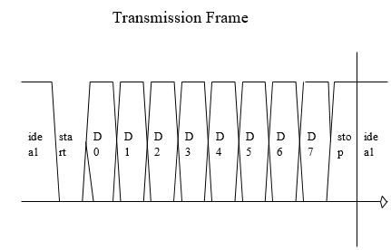
UART (Universal Asynchronous Receiver Transmitter) controller could be a serial communication device. In several control systems, serial communication circuit is employed largely .A universal asynchronous receive/transmit (UART) is an microcircuit which plays the foremost important role in serial communication. Serial communication is differently of communication used widely thanks to its simple structure and long transmission distance. Serial communication is significant to computers and allows them to speak with the low speed devices like keyboard, mouse, modems etc. UARTs are used for serial communication between two devices with minimum wires. the info is shipped serially, and no clock signal is distributed together with it. the first function of a UART is parallel-to-serial conversion when transmitting, and serial to-parallel conversion when receiving. The sender and receiver have separate, unsynchronized, clock signals. so as to synchronize the asynchronous serial data and to insure the information integrity, Start and Stop bits are added to the serial data. The transmitted character consists of an 8- bit data byte, sent LSB (least significant bit) first, preceded by a start bit (active low) and followed by a stop bit (active high). When no character is being transmitted, the road is idle (active high). the road needn't go idle between characters, because it is feasible for the beginning little {bit of} a transmission to right away follow the stop bit of the previous transmission. A field programmable gate array (FPGA) may be a logic device that contains a two dimensional array of generic logic cells and programmable switches. A logic cell will be configured (i.e., programmed) to perform an easy function, and a programmable switch is customized to supply interconnections among the logic cells. A custom design will be implemented by specifying the function of every logic cell and selectively setting the connection of every programmable switch. Once the planning and synthesis are completed, we are able to use a straightforward adaptor cable to download the specified logic cell and switch configuration to the FPGA device and procure the custom circuit.
II. LITERATURE SURVEY
A. UART Transmitter
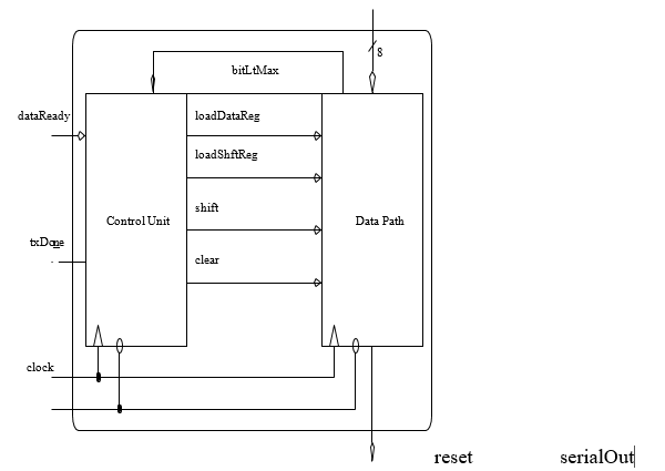
The proposed UART transmitter architecture comprises of two main building blocks which are data path unit and control unit, Figure 4. The architecture of the transmitter data path unit consists of an information register, an information register, and a standing register, which counts the bits that are transmitted. The figure shows the input- output signals of the transmitter. The input signals are provided by the host device, and therefore the output signals are the serial data stream and a standing signal. Data is transmitted serially on the serial Output put. The transmitter is prepared transmit when the status signal txDoneis asserted high. When data Readyis asserted high, the transmitter loads the content of the dataIn into data Register. bitCnt Max indicates the status of the bit counter within the datapath unit.
Functional Block Diagram of the Transmitter
B. UART Receiver
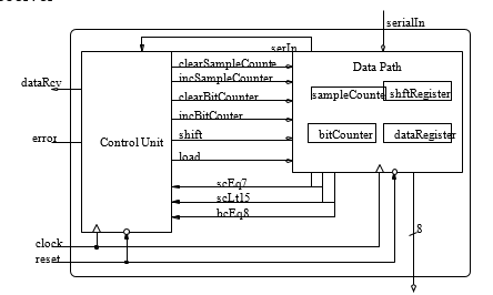
Figure 7 shows a functional diagram of the UART receiver. Data is received serially on the serialIn input. When one byte of knowledge has been received, it's output to the dataOut output bus, and therefore the output control signal dataRcvd is asserted high for one clock period. The block is clocked with a frequency 16 times the information measure.
Functional Block Diagram of the Receiver
C. UART Clock Generator
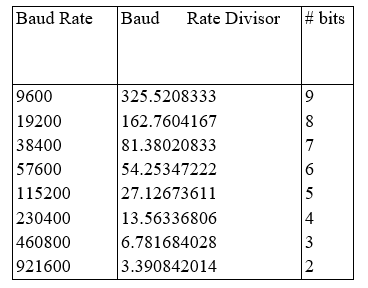
The UART Clock Generator in Figure is accustomed generate UART transmitter clock and receiver sample clock supported the subsequent calculation. the subsequent table shows the baud rate divisor and also the minimum number of bits that are required to store the baud divisor for sample clock.
III. RESULTS AND EVALUATION
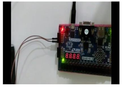
The design of UART is coded using Verilog based top-down hierarchical design methodology and realized in Spartan-3E FPGA using Xilinx ISE Webpack 14.7. Table shows the FPGA utilization for the Microprogrammed implementation of the UART controller compared to the Hardwired implementation. Both implementations use almost the same amount of FPGA resources. However, Microprogrammed implementation operates faster: the minimum clock period of the Microprogrammed implementation is 4.582ns (Maximum Frequency is 218.248MHz) and is 5.187ns (Maximum Frequency is 192.773MHz) for Hardwired implementation. To prove the functionality of our design of UART, we implemented our design in Digilent Basys2 Spartan3E FPGA Board [5]. We then connect the FPGA board to a PC that runs a program that transmits and receives large-size (50 MB to 100 MB) of plain text and binary files. The program then compares the sent bytes to the received bytes. All the bytes that are sent are received correctly.
Comparison of Different Implementations of UART Controller
|
Method |
ROM Size of the transmitter Controller |
||
|
|
Size |
No. of bits |
|
|
ROM method with original SM chart |
16×6 |
96 |
|
|
Microprogram med implementations |
4×8 |
32 |
|
|
Method |
ROM Size of the receiver Controller |
||
|
|
Size |
No. of bits |
|
|
ROM method with original SM chart |
128×1 0 |
1280 |
|
|
Microprogrammed implementations |
7×13 |
91 |
|
Conclusion
In this paper, we have presented FPGA realization of micro programmed implementation of UART controllers. Our design is fully functional and synthesizable and can operate at a maximum clock frequency of 218.248 MHz. The design uses less number of FPGA resources compared to the ROMbased method. In this paper, we have presented FPGA realization of micro programmed implementation of UART controllers. Our design is fully functional and synthesizable on both receiver and transmitting side. We learnt about various new concepts.
References
[1] Alexander Barkalov LT; Logic Synthesis for FSM- Based Control Units. Springer Berlin Heidelberg, 2009. [2] Ali L, Sidek R, Aris I, Ali AM, Suparjo BS; Design of a micro-uart for soc application. Computers & Electrical Engineering, 2004; 30(4):257-268. [3] Barkalov AA, Titarenko LA, Efimenko KN; Optimization of circuits of compositional microprogram control units implemented on fpga. Cybernetics and Sys. Anal, 2011; 47(1):166–174. [4] Bomar BW; Implementation of microprogrammed control in fpgas. Industrial Electronics, IEEE Transactions on, 2002; 49(2): 415–422. [5] Digilent. Digilent Basys2 Spartan-3E FPGA Board. [6] HU Likun WQ; Uart-based reliable communication and performance analysis. In Computer Engineering, 2006; 32: 15–21. [7] Norhuzaimin J, Maimun H; The design of high speed uart. In Applied Electromagnetics, APACE 2005. Asia-Pacific Conference on, 2005. [8] Roth Jr. CH, John LK; Digital Systems Design Using VHDL. Thomson-Engineering, 2007. [9] Tomasi W; Advanced electronic communication systems, Third Edition. Prentice-Hall, 1994. [10] Wis´niewski R, Barkalov A, Titarenko L, Halang W; Design of microprogrammed controllers to be implemented in fpgas. Int. J. Appl. Math. Comput. Sci, 2011; 21(2):401– 412. [11] Yi-yuan F, Xue-jun C; Design and simulation of uart serial communication module based on vhdl. In Intelligent Systems and Applications (ISA), 2011 3rd International Workshop on, 2011; 1-4.
Copyright
Copyright © 2022 Anchal Govil, Anmol Karnwal, Govinda Sindhu, Ayush Singh, Dr. Shubham Shukla . This is an open access article distributed under the Creative Commons Attribution License, which permits unrestricted use, distribution, and reproduction in any medium, provided the original work is properly cited.

Download Paper
Paper Id : IJRASET41478
Publish Date : 2022-04-14
ISSN : 2321-9653
Publisher Name : IJRASET
DOI Link : Click Here
 Submit Paper Online